Structure of surface-modified silver-palladium alloy wire

A surface modification, silver-palladium alloy technology, applied in semiconductor/solid-state device parts, semiconductor devices, electrical components, etc., can solve problems such as many restrictions

Inactive Publication Date: 2016-02-10
TANAKA DENSHI KOGYO KK
View PDF14 Cites 2 Cited by
  • Summary
  • Abstract
  • Description
  • Claims
  • Application Information

AI Technical Summary

Problems solved by technology

[0013] This is because the bonding conditions of bonding wires for thin wires using an ultrasonic device depend on frequency (about tens to hundreds of kHz), output (about several W at the maximum) and pressure (about several tens of gf), so , which is more restrictive than the bonding condition for the first bonding

Method used


Image

  • Structure of surface-modified silver-palladium alloy wire
  • Structure of surface-modified silver-palladium alloy wire
  • Structure of surface-modified silver-palladium alloy wire

Examples


Embodiment

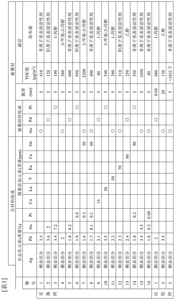
[0060] The silver-palladium alloy (silver (Ag), gold (Au) and copper (Cu) with a purity of 99.9999% by mass or more of the composition of the core material and the coating material in Table 1, and other palladium (Pd) and platinum (Pt) The alloying components of the alloys have a purity of 99.999% by mass or more), melt-casting uniformly, rolling while performing intermediate heat treatment (600°C×0.5 hours), and then drawing to obtain a thick wire (diameter 0.5mm) before coating the coating material.

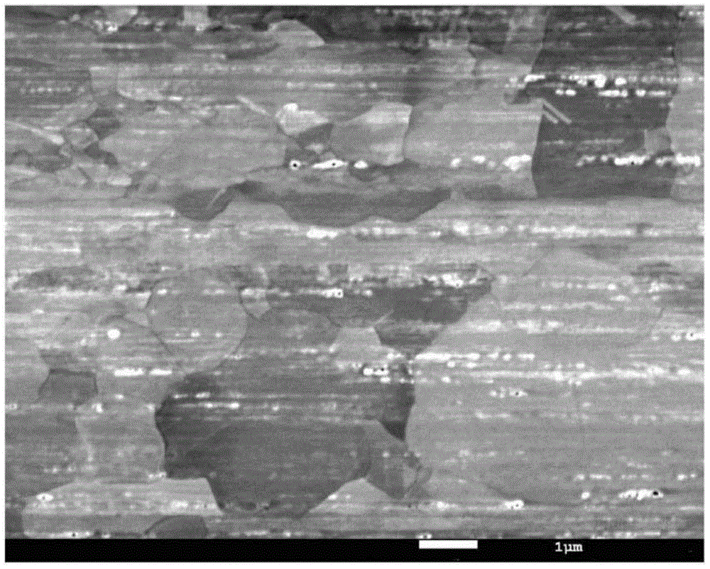
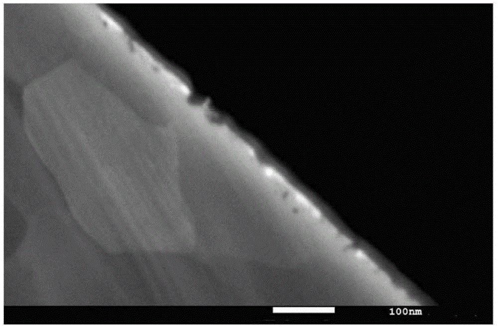
[0061] A core material composed of an Ag-3.5% by mass Pd alloy shown in No. 1 in Table 1 was drawn to a diameter of 0.5 mm, and the outer circumference of the thick wire was coated with gold (Au) at a thickness of about 0.1 μm. Thereafter, the wire was continuously drawn using a diamond die in a wet method to finally obtain a wire for ultrasonic bonding with a diameter of 15 μm. The structure of the plane obtained by observing the appearance of the line with a scanning electron...


PUM

PropertyMeasurementUnit
thicknessaaaaaaaaaa
diameteraaaaaaaaaa
diameteraaaaaaaaaa

Abstract

The invention relates to a structure of a surface-modified silver-palladium alloy wire. The surface-modified silver-palladium alloy wire is composed of a core and a surface-modified layer. The core is made of Ag-Pd alloy or Ag-Pd-Au(Pt) alloy prepared from Ag and Au respectively with the purity being more than 99.99 mass% and Pd with the purity being more than 99.9 mass%, wherein the mass ratio of the Ag and Pd of the Ag-Pd alloy is 100:(1-5), and the mass ratio of the Ag, Pd and Au(or Pt)of the Ag-Pd-Au(Pt) alloy is 100:(1-5):(0.05-10). The surface-modified layer is composed of Ag, Pd and Pt respectively with the purity being more than 99.99 mass% and alloys thereof. The structure of the surface-modified silver-palladium alloy wire is characterized in that the wire surface and the grain boundary of the core form cross dark rings with the interval being 20-30 [mu]m in the long side direction of the wire, and the surface morphology of the surface-modified layer is embedded in uneven-sized longitudinal grooves of the core.

Description

technical field [0001] The present invention relates to a surface-modified silver-palladium alloy bonding wire suitable for connecting IC chip electrodes used in semiconductor devices to substrates such as external leads, and in particular to ultrasonic waves used in high-temperature environments such as automotive applications, power semiconductors, and high-speed equipment applications. Bonding and bump wires for connection, or surface-modified silver bonding wires for air-free balls (FAB) that can be used even with ultra-thin wires of 15 μm or less. Background technique [0002] Conventionally, various kinds of silver-palladium alloy bonding wires for connecting IC chip electrodes and external leads of semiconductor devices have been developed. For example, it is a bonding wire "containing 1 to 30 wt% of Pd in ​​Ag" (Japanese Patent Application Laid-Open No. 57-021830), "at least 1 of Pd added to Ag in a total of 500 to 3000 wt% "bonding wire" (Japanese Patent Applicatio...

Claims


Application Information

Patent Timeline
Patent Type & Authority Applications(China)
IPC IPC(8): H01L23/49
CPCH01L24/45H01L2224/45015H01L2224/45139H01L2224/45565H01L2224/45644H01L2224/45664H01L2224/45669H01L2224/45014H01L2224/05624H01L2924/00011H01L2924/00014H01L2224/45H01L2924/01046H01L2924/01204H01L2924/0102H01L2924/01057H01L2924/01063H01L2924/01058H01L2924/01032H01L2924/01205H01L2924/20751H01L2924/00012H01L2924/01049H01L2924/206
Inventor 三上道孝刘斌安原和彦千叶淳冈崎纯一前田菜那子
Owner TANAKA DENSHI KOGYO KK
Why Eureka
Try Eureka