Isolation trench film filling structure, semiconductor memory device and preparation method

A technology for isolating trenches and storage devices, which is applied in semiconductor/solid-state device manufacturing, electrical components, circuits, etc. It can solve problems such as easy generation of voids, device failure, and short circuit of metal bit lines, so as to reduce the generation of voids and improve good quality. rate, the effect of expanding the opening aperture

Pending Publication Date: 2018-02-16
CHANGXIN MEMORY TECH INC
View PDF5 Cites 2 Cited by
  • Summary
  • Abstract
  • Description
  • Claims
  • Application Information

AI Technical Summary

Problems solved by technology

[0008] In view of the above-mentioned shortcomings of the prior art, the object of the present invention is to provide an isolation trench film filling structure, a semiconductor storage device and a preparation method, which are used to so

Method used


Image

  • Isolation trench film filling structure, semiconductor memory device and preparation method
  • Isolation trench film filling structure, semiconductor memory device and preparation method
  • Isolation trench film filling structure, semiconductor memory device and preparation method

Examples


Embodiment Construction

[0064] Embodiments of the present invention are described below through specific examples, and those skilled in the art can easily understand other advantages and effects of the present invention from the content disclosed in this specification. The present invention can also be implemented or applied through other different specific implementation modes, and various modifications or changes can be made to the details in this specification based on different viewpoints and applications without departing from the spirit of the present invention.

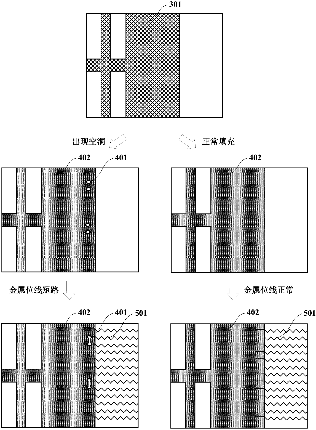
[0065] In the background technology, for figure 1 The problem of voids 401 appearing in the present invention, the inventors have found through in-depth research that the reason why voids 401 often appear between the prefabricated filling layer 301 and the high-density plasma oxide layer 402 is that after the prefabricated filling material is formed on the semiconductor substrate 100 ,Such as figure 2 and image 3 As shown, the pre...


PUM


Abstract

The invention provides an isolation trench film filling structure, a semiconductor memory device and a preparation method. The preparation method of the isolation trench film filling structure comprises the steps that a semiconductor substrate with a peripheral groove is provided; a prefabricated filling material is formed on the semiconductor substrate, and the upper surface of the semiconductorsubstrate and the sidewall and the bottom of the peripheral groove are covered to form a neck; the prefabricated filling material is pre-etched to remove the neck; a high-density plasma oxide materialis formed on the semiconductor substrate; the prefabricated filling material is covered, and the peripheral groove is filled; and extra high-density plasma oxide material and prefabricated filling material are removed to acquire a high-density plasma oxide material layer and a prefabricated filling layer in the peripheral groove. According to the invention, the shape of the prefabricated fillinglayer is improved through pre-etching; voids between the high-density plasma oxide material and the prefabricated filling material are prevented; and device failure caused by short circuit caused by asubsequently formed metal bit line is prevented.

Description

technical field [0001] The invention relates to the technical field of semiconductors, in particular to an isolation trench film filling structure, a semiconductor storage device and a preparation method. Background technique [0002] Patterning can generate topological shapes with three spatial dimensions on the wafer surface, which form gaps and steps on the wafer surface. A small gap (such as an isolation trench or via) can be described by an aspect ratio, which is defined as the ratio of the depth to the width of the gap. In device fabrication, the ability to fill small gaps on the silicon wafer surface becomes the most important film property. For small gaps, high / low aspect ratios make it difficult to deposit films with uniform thickness, and pinch-offs and voids can occur. With the continuous reduction of the feature size of high-density integrated circuits, it is very important to perform a uniform and void-free filling deposition process for gaps with high / low asp...

Claims


Application Information

Patent Timeline
IPC IPC(8): H01L21/762
CPCH01L21/76224H01L21/76229
Inventor 不公告发明人
Owner CHANGXIN MEMORY TECH INC
Why Eureka
Try Eureka