Three-dimensional photoelectric integrated structure and preparation method thereof
An optoelectronic integrated, three-dimensional technology, applied in circuits, electrical components, electrical solid devices, etc., can solve the problems of poor heat dissipation performance, complex process, poor performance of photonic chips, etc., to improve heat dissipation effect, simple process, and solve problems with poor performance. Effect
- Summary
- Abstract
- Description
- Claims
- Application Information
AI Technical Summary
Problems solved by technology
Method used
Image

Examples
Embodiment 1
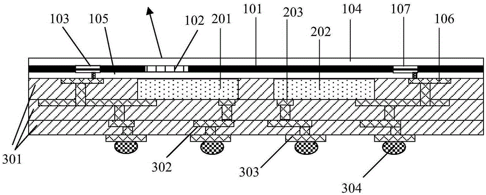
[0043] In order to solve the technical problems of poor performance, complex process and poor heat dissipation performance of the photonic chip caused by the integration technology in the prior art, the present application provides a three-dimensional optoelectronic integrated structure. Such as figure 1 As shown, the three-dimensional optoelectronic integrated structure includes: an optoelectronic chip, a rewiring medium, electronic devices 202 and 201, an optical fiber 108, and a substrate 401.
[0044] The optoelectronic chip includes a buried oxygen layer 104, a top layer interconnection medium 105, a top layer silicon 101, a back reflection grating 102, and photonic devices 103 and 107. The top silicon 101 is disposed between the buried oxide layer 104 and the top interconnection medium 105, the photonic devices 103 and 107 are disposed in the top silicon 101, and the photonic device pads 106 of the photonic devices 103 and 107 are disposed on the On the top-level interconne...
Embodiment 2
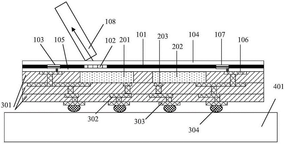
[0052] Based on the same inventive concept, the present application also provides a method for manufacturing a three-dimensional optoelectronic integrated structure. The manufacturing method is used for manufacturing the three-dimensional optoelectronic integrated structure in the first embodiment. Such as figure 2 As shown, the manufacturing method includes the following steps:
[0053] Step S110, such as image 3 As shown, the optoelectronic chip is obtained, and the optoelectronic chip includes a buried oxide layer 104, a top layer interconnection medium 105, a top layer silicon 101, a back reflection grating 102, and photonic devices 103 and 107. The top silicon 101 is disposed between the buried oxide layer 104 and the top interconnection medium 105, the photonic devices 103 and 107 are disposed in the top silicon 101, and the pins of the photonic devices 103 and 107 pass through the top interconnection Medium 105. A silicon substrate 109 is provided on the buried oxygen l...
PUM
 Abstract
Description
Claims
Application Information
 - Generate Ideas
- Intellectual Property
- Life Sciences
- Materials
- Tech Scout
- Unparalleled Data Quality
- Higher Quality Content
- 60% Fewer Hallucinations
Browse by: Latest US Patents, China's latest patents, Technical Efficacy Thesaurus, Application Domain, Technology Topic, Popular Technical Reports.
© 2025 PatSnap. All rights reserved.Legal|Privacy policy|Modern Slavery Act Transparency Statement|Sitemap|About US| Contact US: help@patsnap.com