

Wafer chuck cleaning system used for lithography machine and cleaning method thereof
A cleaning system and lithography machine technology, applied in the semiconductor field, can solve the problems of grinding stone loss, damage to the closed chamber environment, secondary pollution, etc., and achieve the effects of low cost, avoiding repeated pollution, and small changes
- Summary
- Abstract
- Description
- Claims
- Application Information
AI Technical Summary
Problems solved by technology
Method used
Image

Examples
Embodiment Construction
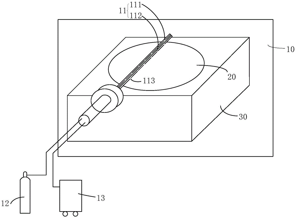
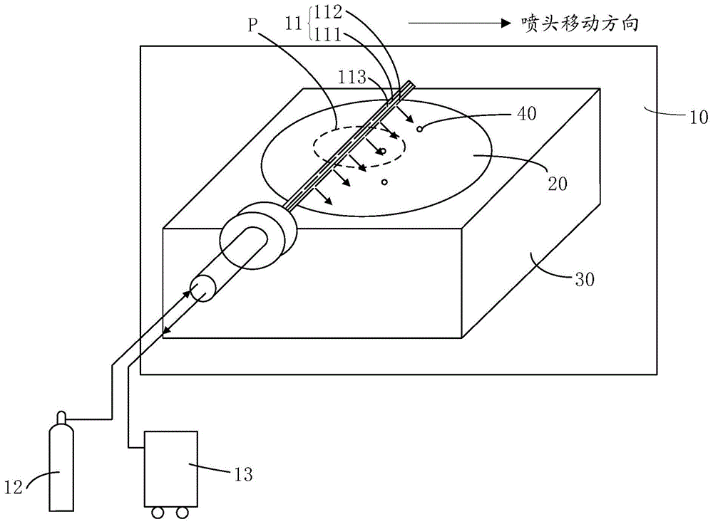
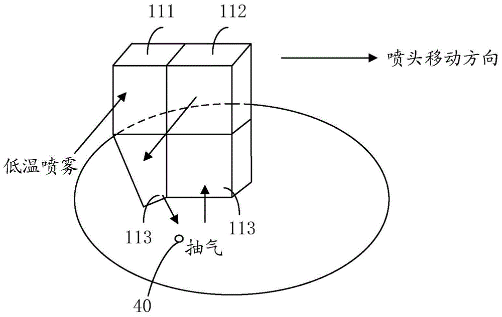
[0048]As mentioned in the background technology, the existing wafer chuck cleaning method does not need to open the closed chamber where the wafer chuck is located, and remove the chuck to remove pollutants, which will destroy the environment of the closed chamber and take time. ; Or use a grinding stone to grind the surface of the wafer chuck in a closed chamber, but this will damage the surface of the wafer chuck. In view of the above technical problems, the present invention proposes to install a spray head in the closed chamber where the wafer chuck is located. The above spray head provides a low-temperature spray to the surface of the wafer chuck when it needs to be cleaned. The above-mentioned low-temperature spray is particles with a certain quality, carrying At a certain speed, it can collide with the pollutants on the surface of the wafer chuck, so that the above-mentioned pollutants are separated from the surface of the chuck, and at the same time, the air extraction ...
PUM
| Property | Measurement | Unit |
|---|---|---|
| length | aaaaa | aaaaa |
Abstract
Description
Claims
Application Information