Formation method of transistor

A technology of transistors and semiconductors, applied in semiconductor devices, semiconductor/solid-state device manufacturing, electrical components, etc., can solve problems affecting transistor performance, affecting metal layer filling, and increasing difficulty of work function layers, achieving high trench filling capabilities, Improved performance, high interface quality effects

Active Publication Date: 2016-02-17
SEMICON MFG INT (SHANGHAI) CORP
View PDF5 Cites 14 Cited by
  • Summary
  • Abstract
  • Description
  • Claims
  • Application Information

AI Technical Summary

Problems solved by technology

[0004] As the process node decreases, the size of the groove formed after removing the dummy gate structure is further reduced, making it more difficult to form a work function layer in the groove. In the process of forming the work function layer by physical vapor deposition process , it is easy to have a sealing phenomenon at the opening of the groove, which affects the filling of the subsequent metal layer, thereby affecting the performance of the transistor

Method used


Image

  • Formation method of transistor
  • Formation method of transistor
  • Formation method of transistor

Examples


Embodiment Construction

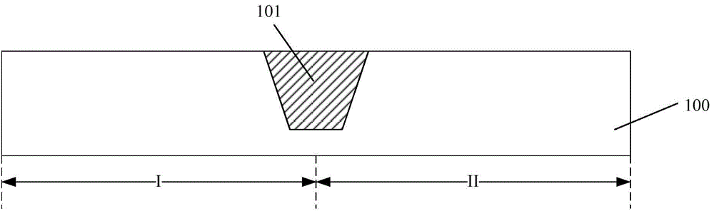
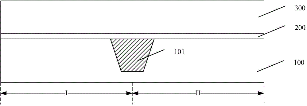
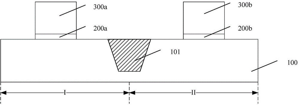
[0027] As mentioned in the background art, in the prior art, the deposition quality of the work function layer formed by the physical vapor deposition process in the groove is poor, which may easily cause the top of the groove to be closed and affect the performance of the formed transistor.

[0028] Research has found that the work function layer can be formed by using an atomic layer deposition process with higher groove filling performance instead of the physical vapor deposition process.

[0029] However, further studies have found that although the atomic layer deposition process is used to form the work function layer, which has a high groove filling ability and will not cause the top of the groove to be closed, it is found in the process of forming the NMOS work function layer that the atomic layer The deposition quality of the NMOS work function layer formed by the deposition process and the quality of the interface with adjacent layers (for example: protective layer) a...


PUM

PropertyMeasurementUnit
thicknessaaaaaaaaaa
thicknessaaaaaaaaaa
thicknessaaaaaaaaaa

Abstract

The invention discloses a formation method of a transistor. The method comprises the following steps: providing a semiconductor substrate including a first area, wherein a dielectric layer is formed on the surface of the semiconductor substrate, and the dielectric layer is internally provided with a first groove exposing a part of the surface of the first area of the semiconductor substrate; forming a gate medium material layer on the surface of the inner wall of the first groove and the dielectric layer; forming a protective material layer on the gate medium material layer; forming an adherence material layer on the protective material layer by use of a physical vapor deposition technology; forming a first work function material layer by use of an atomic layer deposition technology, wherein the material of the adherence material layer is the same as the material of the first work function material layer; forming a grid metal layer on the first work function material layer, wherein the grid metal layer fills up the groove; and performing planarization processing on the grid metal layer, the first work function material layer, the adherence material layer, the protective material layer and the grid medium material layer by taking the surface of the dielectric layer as a stop layer so as to form a first grid structure disposed in the first groove. The method provided by the invention can improve the performance of the transistor.

Description

technical field [0001] The invention relates to the technical field of semiconductors, in particular to a method for forming a transistor. Background technique [0002] With the continuous improvement of the integration level of semiconductor devices and the reduction of technology nodes, the traditional gate dielectric layer continues to become thinner, and the leakage of transistors increases accordingly, causing problems such as waste of power consumption of semiconductor devices. In order to solve the above problems, the prior art provides a solution of replacing the polysilicon gate with a metal gate. Among them, the "gate last" process is a main process for forming high-K metal gate transistors. [0003] The existing method for forming a high-K metal gate transistor using a gate-last process includes: providing a semiconductor substrate on which a dummy gate structure is formed and located on the semiconductor substrate and covering the dummy gate structure The diele...

Claims


Application Information

Patent Timeline
Patent Type & Authority Applications(China)
IPC IPC(8): H01L21/28H01L21/285H01L21/336
Inventor 徐建华
Owner SEMICON MFG INT (SHANGHAI) CORP
Why Eureka
Try Eureka