Deep hole bottom windowing etching method of silicon through hole

A technology of through-silicon vias and deep holes, which is applied in the fields of electrical components, semiconductor/solid-state device manufacturing, circuits, etc., can solve the problems of low selection ratio and easy short circuit, achieve high mask etching selection ratio, and the method design is simple and reasonable Effect

Active Publication Date: 2016-02-17
BEIJING NAURA MICROELECTRONICS EQUIP CO LTD
View PDF4 Cites 0 Cited by
  • Summary
  • Abstract
  • Description
  • Claims
  • Application Information

AI Technical Summary

Problems solved by technology

[0007] Based on this, it is necessary to provide a deep hole bottom opening etching method with fast etching rate and high selective ratio for TSV deep hole etching, such as easy short circuit and low selectivity ratio.

Method used


Image

  • Deep hole bottom windowing etching method of silicon through hole
  • Deep hole bottom windowing etching method of silicon through hole
  • Deep hole bottom windowing etching method of silicon through hole

Examples


Embodiment Construction

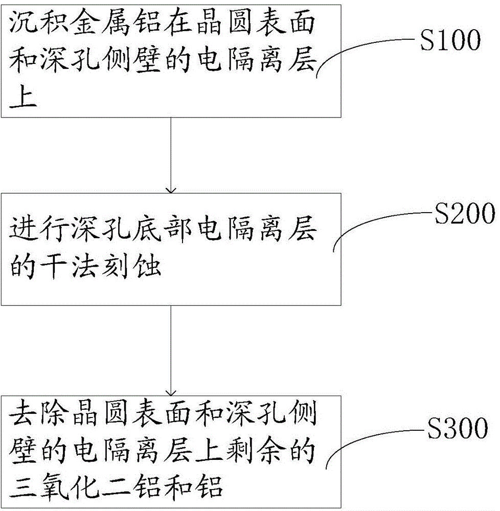
[0032] In order to make the object, technical solution and advantages of the present invention clearer, the method for etching the deep hole bottom of the through-silicon via according to the present invention will be further described in detail through the following examples and in conjunction with the accompanying drawings. It should be understood that the specific embodiments described here are only used to explain the present invention, not to limit the present invention.

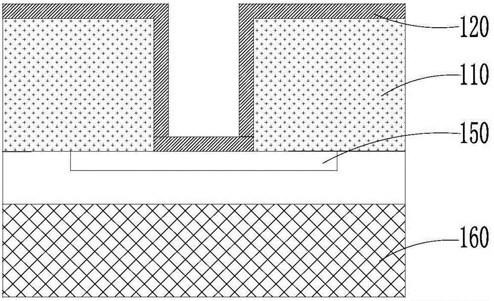
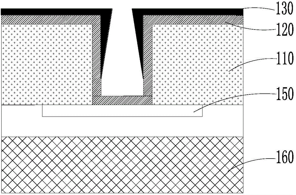
[0033] see Figure 3 to Figure 7 , the etching method for opening a window at the bottom of a deep hole of the through-silicon via of the present invention, comprising the following steps:

[0034] S100, deposit metal aluminum 130 on the surface of the wafer and the electrical isolation layer 120 on the sidewall of the deep hole;

[0035] S200, performing dry etching of the electrical isolation layer 120 at the bottom of the deep hole, including the following two steps:

[0036] S210, oxidation step, ...


PUM


Abstract

The invention provides a deep hole bottom windowing etching method of a silicon through hole. The method comprises the following steps of depositing metal aluminum electrical isolation layers of a wafer surface and a deep hole side wall; carrying out dry method etching of a deep hole bottom electrical isolation layer, wherein the above step comprises two steps of an oxidation step: carrying out metal aluminum oxidation reaction so as to form aluminum oxide; an etching step: using a technology gas to carry out etching; repeating the oxidation step and the etching step till that the electrical isolation layer of the deep hole bottom is completely removed; and removing the residual aluminum oxide and aluminum on the electrical isolation layer of the wafer surface. By using the deep hole bottom windowing etching method of the silicon through hole, the method is designed simply and reasonably; a simple film deposition, oxidation and etching technology is used and a high electrical isolation layer / mask etching selection ratio is acquired.

Description

technical field [0001] The invention relates to the technical field of semiconductor manufacturing, in particular to an etching method for opening a window at the bottom of a deep hole of a through-silicon hole. Background technique [0002] The three-dimensional stacked integrated circuit packaging technology based on TSV technology (TSV, ThroughSiliconVia) is the latest packaging technology. It has the smallest size and quality, effectively reduces parasitic effects, improves chip speed and reduces power consumption. TSV technology is The latest technology for interconnection between chips is realized by making vertical conduction between chips, so TSV technology can make packaged products have a higher structural density, thereby achieving more functions and superior performance while maintaining more low cost. [0003] To achieve TSV packaging, it generally includes the following processes: 1. Wafer thinning to meet the requirements of small packaging thickness; 2. Bond...

Claims


Application Information

Patent Timeline
IPC IPC(8): H01L21/768H01L21/3213H01L21/311
Inventor 周娜蒋中伟
Owner BEIJING NAURA MICROELECTRONICS EQUIP CO LTD
Why Eureka
Try Eureka