Polycrystalline diamond compact and manufacturing method thereof
A technology of polycrystalline diamond and composite sheet, which is applied in metal material coating process, gaseous chemical plating, coating, etc., which can solve the problems of poor wear resistance of composite sheet, larger Co volume, and increased distortion energy. , to achieve the effect of prolonging the service life, increasing the total surface area, and enhancing the anti-coating peeling ability
- Summary
- Abstract
- Description
- Claims
- Application Information
AI Technical Summary
Problems solved by technology
Method used
Image
Examples
Embodiment 1
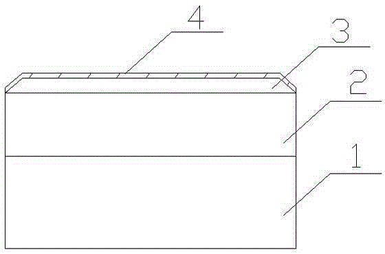
[0039] A polycrystalline diamond composite sheet, such as figure 1 with Figure 4 As shown, it includes a cylindrical composite sheet substrate and a working end surface 3. The composite sheet substrate includes a cemented carbide base layer 1 and a polycrystalline diamond layer 2 covered on the upper surface of the cemented carbide base layer 1, a cemented carbide base layer 1 and a polycrystalline diamond layer 2 It is sintered into a whole through high temperature and high pressure; the working end face 3 is located on the upper end face of the polycrystalline diamond layer 2, and the working end face 3 is coated with a multilayer nano-diamond layer 4, and the total thickness of the multilayer nano-diamond layer 4 is 6 μm.
[0040] Each nano-diamond layer 4 includes a nanocrystalline layer 5 with an average grain size of 20 nm and a nanocrystalline layer 6 with an average grain size of 60 nm. The thickness of each nanocrystalline layer is 0.3um.
[0041] The preparation method i...
Embodiment 2
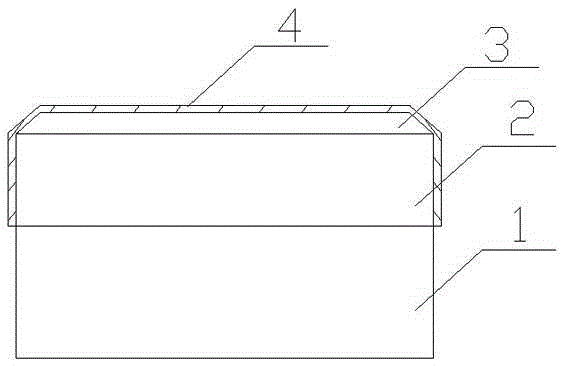
[0052] Such as figure 2 As shown, in this embodiment, the working end surface of the composite sheet substrate and the side surface of the polycrystalline diamond layer are both coated with multiple nano-diamond layers. The total thickness of the multiple nano-diamond layers 4 is 16 μm, and each nano-diamond layer 4 It includes two nanocrystalline layers with an average grain size of 40nm and 60nm respectively. The thickness of each nanocrystalline layer is 0.4um. The rest is the same as in Example 1.
[0053] The preparation method includes the following steps:
[0054] (1) Preparation of the composite sheet substrate: mix the diamond powder and the binder, and sinter with the hard aluminum alloy substrate at 5.5GPa, 1400°C for 8 minutes to obtain the composite sheet substrate blank. The composite sheet substrate blank is processed by grinding and finishing. After treatment, a composite sheet substrate blank with a polycrystalline diamond layer on the upper surface of the cemen...
Embodiment 3
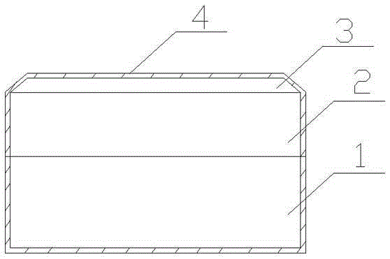
[0064] In this embodiment, such as image 3 As shown, the working end surface of the polycrystalline diamond layer and the side surface of the composite sheet substrate are both coated with a multilayer nano-diamond layer 4, and the total thickness of the multilayer nano-diamond layer 4 is 20 μm. Each nano-diamond layer 4 includes two nano-crystalline layers with an average crystal grain size of 40 nm and 80 nm, respectively. The rest is the same as in Example 1.
[0065] The preparation method includes the following steps:
[0066] (1) Preparation of composite sheet: Mix diamond powder and binder, and sinter with hard aluminum alloy matrix at 5.5GPa, 1550℃ for 6min to obtain the composite sheet base blank, and the composite sheet base blank is processed by grinding and finishing. Afterwards, a composite sheet substrate blank with the upper surface of the cemented carbide base layer covered with a polycrystalline diamond layer is obtained. The composite sheet substrate blank is pr...
PUM
| Property | Measurement | Unit |
|---|---|---|
| Total thickness | aaaaa | aaaaa |
| Average grain size | aaaaa | aaaaa |
| Average grain size | aaaaa | aaaaa |
Abstract
Description
Claims
Application Information


