

Binding gold finger compensation method
A compensation method, finger technology, applied in the direction of electrical connection formation of printed components, electrical components, printed circuit liquid treatment, etc., can solve the problem that the effective area of welding cannot be satisfied
- Summary
- Abstract
- Description
- Claims
- Application Information
AI Technical Summary
Problems solved by technology
Method used
Image

Examples
Embodiment Construction
[0014] The invention provides a binding gold finger compensation method, which includes the following steps: S1: drilling, S2: copper plating, S3: dry film pretreatment, S4: pattern transfer, S5: line etching-DES, S6: AOI Inspection, S7: Printing solder mask (including pre-treatment), S8: Surface treatment, S9: Forming, S10: Electrical testing, S11: Finished product inspection-FQC.
[0015] The above-mentioned step S4: the technological process of pattern transfer is followed by dry film pressing and circuit exposure.
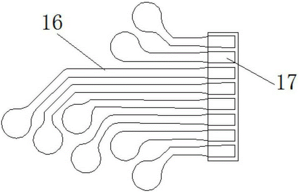
[0016] Such as figure 1 The step S5 shown: line etching-DES is to slow down the speed of liquid medicine exchange in the gap by reducing the gap between the adjacent line rear ends 17 under the premise that the line front end 16 remains unchanged, so that the etched line The rear end 17 is at a right angle, thereby ensuring that the area of the binding fingers after etching is consistent with the area of the binding fingers before etching.
[0017] The ab...
PUM
 Abstract
Description
Claims
Application Information