PMOS structure and formation method thereof

A gate structure, silicon germanium technology, applied in the direction of electrical components, semiconductor/solid-state device manufacturing, circuits, etc., can solve the hot carrier injection effect and the deterioration of negative bias temperature instability, the increase of PMOS gate current, Reduce the stability of the device and other problems, achieve the effect of improving the hot carrier injection effect, improving stability, and reducing the probability of diffusion

Inactive Publication Date: 2016-03-02
SEMICON MFG INT (SHANGHAI) CORP
View PDF3 Cites 3 Cited by
  • Summary
  • Abstract
  • Description
  • Claims
  • Application Information

AI Technical Summary

Problems solved by technology

[0005] The problem to be solved by the present invention is that when the embedded silicon germanium layer of PMOS structure is formed, the in-situ doped boron ion diffuses into the channel to cause the PMOS gate current to increase and the electrical performance to decrease, and the embedded silicon germanium layer Diffusion of germanium ions leads to deterioration of hot carrier injection effect and negative bias temperature instability, resulting in a decrease in device stability

Method used


Image

  • PMOS structure and formation method thereof
  • PMOS structure and formation method thereof
  • PMOS structure and formation method thereof

Examples


Embodiment Construction

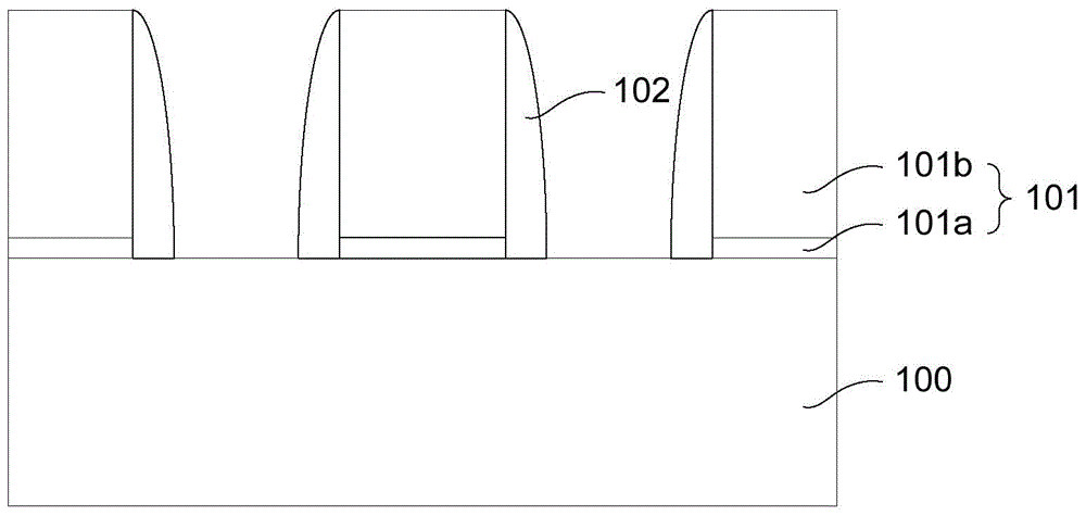
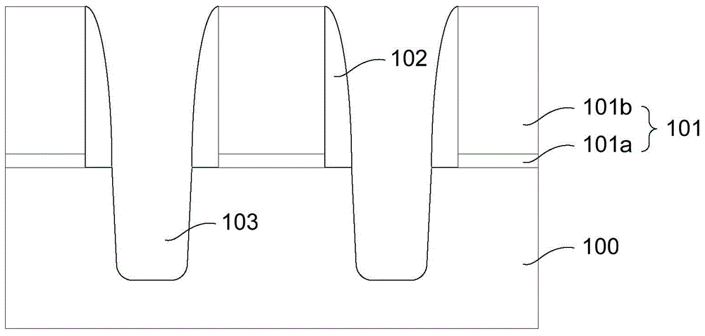
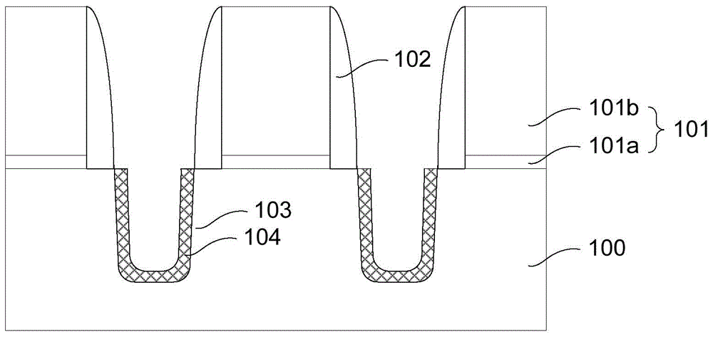
[0032] It can be seen from the background art that the PMOS structure formed by the prior art process has the problems of electrical performance drift and electrical performance degradation. For this reason, the semiconductor device and its formation process were studied, and it was found that when the embedded silicon germanium layer is formed by selective epitaxial growth in the PMOS source and drain regions, the in-situ doped boron ions will diffuse in the subsequent annealing process , increasing the gate current leads to a drift in the electrical performance of the PMOS. The germanium ions in the germanium-silicon layer will also diffuse into the channel, which not only changes the hole mobility rate, but also changes the total charge quantity in the channel, resulting in the deterioration of the hot carrier injection effect and negative bias temperature instability. , greatly reducing the electrical performance of the PMOS.

[0033] In order to solve the above problems,...


PUM

PropertyMeasurementUnit
Doping concentrationaaaaaaaaaa

Abstract

The invention provides a PMOS structure and a formation method thereof. The formation method of the PMOS structure includes: a semiconductor substrate is provided, and a grid electrode structure and side walls positioned on sidewalls of two sides of the grid electrode structure are formed on the surface of the semiconductor substrate; the grid electrode structure and the side walls are regarded as masks, and grooves are formed at two sides of the side walls in the semiconductor substrate; germanium silicon seeding layers are formed on the surfaces of the bottom surfaces and side surfaces of the grooves, and the germanium silicon seeding layers are doped with fluorinions; and silicon germanium body layers are formed on the silicon germanium seeding layers, and remaining portions of the grooves are filled with the silicon germanium body layers. The fluorinions and silicon have strong bonding force, the germanium silicon seeding layers are doped with the fluorinions so that the transferred electron effect can be reduced, and the diffusion of P-type ions is prevented; besides, through the doping of the fluorinions, the stability of the device can be improved, and the negative bias temperature instability and the hot carrier injection effect are improved.

Description

technical field [0001] The invention relates to the field of semiconductors, in particular to a PMOS structure and a forming method thereof. Background technique [0002] With the rapid development of integrated circuit manufacturing technology, the technology nodes of semiconductor devices are constantly decreasing, and the geometric dimensions of devices are also shrinking continuously following Moore's law. When the size of the semiconductor device is reduced to a certain extent, various problems caused by the semiconductor device approaching the physical limit appear one after another. The conventional source-drain region structure has been unable to meet the increasingly high requirements for device operation speed, so Embedded SiGe technology (EmbeddedSiGetechnology) to improve the electrical performance of PMOS has emerged. This technology embeds a silicon germanium layer in the substrate of the PMOS source and drain regions, and uses the stress generated by the latt...

Claims


Application Information

Patent Timeline
IPC IPC(8): H01L21/336H01L21/20H01L29/78H01L29/06
Inventor 李凤莲
Owner SEMICON MFG INT (SHANGHAI) CORP
Why Eureka
Try Eureka