Tensile pressure sensor based on printed transparent electrodes and preparation method thereof
A pressure sensor and transparent electrode technology, applied in the field of sensors, can solve problems affecting the practicality and user experience of bionic electronic skin, limit applications, and high cost, and achieve high sensitivity and stability, good electrical connection, and low cost.
- Summary
- Abstract
- Description
- Claims
- Application Information
AI Technical Summary
Problems solved by technology
Method used
Image
Examples
Embodiment 1
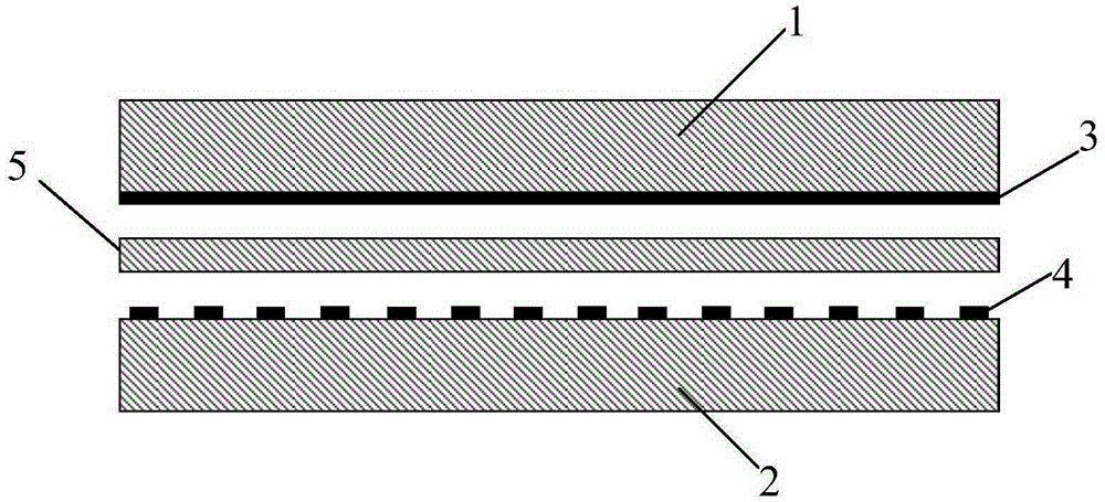
[0069] (1) Fully mix the commercially available PDMS monomer and curing agent (DowCorning, SYLGARD184, the United States) according to the mass ratio of 10:1, and use OSP-100 Meyer rod (OSP-100, Shijiazhuang OSP Machinery Technology Co., Ltd. company) on the surface of commercially available inkjet printing photo paper (Canon, LU-101 professional suede photo paper, Japan), and then placed in a vacuum oven at room temperature for 5 minutes to remove air bubbles in the coating, and then cured at 70 ° C 2 hours, and peeled off from the photo paper surface to obtain a stretchable substrate with a thickness of 100 μm. Using the same method, an OSP-20 Meyer rod (OSP-20, Shijiazhuang OSP Machinery Technology Co., Ltd.) was used for coating to obtain a dielectric layer with a thickness of 20 μm.
[0070] (2) Synthesize and prepare silver nanoparticles (refer to the following literature: Li Weiwei, Mo Lixin, Fu Jilan, etc., Simple method and characterization of crystal form-controlled ...
Embodiment 2
[0077] (1) Fully mix the commercially available PDMS monomer and curing agent (DowCorning, SYLGARD184, the United States) according to the mass ratio of 10:1, and use OSP-1.5 Meyer rod (OSP-1.5, Shijiazhuang OSP Machinery Technology Co., Ltd. company) on the surface of commercially available inkjet printing photo paper (Canon, LU-101 professional suede photo paper, Japan), and then placed in a vacuum oven at room temperature for 5 minutes to remove air bubbles in the coating, and then cured at 70 ° C 2 hours, and peeled off from the surface of the photo paper to obtain a stretchable substrate and a dielectric layer, wherein the thickness of the stretchable substrate is 1 μm, and the thickness of the dielectric layer is 1 μm.
[0078] (2) Synthesize and prepare silver nanoparticles (refer to the following literature: Li Weiwei, Mo Lixin, Fu Jilan, etc., Simple method and characterization of crystal form-controlled nano-silver synthesis, Rare Metal Materials and Engineering, 2013...
Embodiment 3
[0084] (1) Fully mix the commercially available PDMS monomer and curing agent (DowCorning, SYLGARD184, the United States) according to the mass ratio of 10:1, and use OSP-50 Meyer rod (OSP-50, Shijiazhuang OSP Machinery Technology Co., Ltd. company) on the surface of commercially available inkjet printing photo paper (Canon, LU-101 professional suede photo paper, Japan), and then placed in a vacuum oven at room temperature for 5 minutes to remove air bubbles in the coating, and then cured at 70 ° C 2 hours, and peeled off from the photo paper surface to obtain a stretchable substrate with a thickness of 50 μm. Using the same method, an OSP-10 Meyer rod (OSP-10, Shijiazhuang OSP Machinery Technology Co., Ltd.) was used for coating to obtain a dielectric layer with a thickness of 10 μm.
[0085] (2) Synthesize and prepare silver nanoparticles (refer to the following literature: Li Weiwei, Mo Lixin, Fu Jilan, etc., Simple method and characterization of crystal form-controlled nan...
PUM
| Property | Measurement | Unit |
|---|---|---|
| thickness | aaaaa | aaaaa |
| thickness | aaaaa | aaaaa |
| particle diameter | aaaaa | aaaaa |
Abstract
Description
Claims
Application Information


