Manufacturing method of pnbzt film

A manufacturing method and thin-film technology, which is applied in chemical instruments and methods, semiconductor/solid-state device manufacturing, niobium compounds, etc., can solve problems such as the decrease of piezoelectric properties of PNbZT thin films, and achieve a roughly uniform composition distribution

Active Publication Date: 2018-07-06
MITSUBISHI MATERIALS CORP
View PDF2 Cites 0 Cited by
  • Summary
  • Abstract
  • Description
  • Claims
  • Application Information

AI Technical Summary

Problems solved by technology

[0005] However, in the technique for improving the piezoelectric properties of PZT thin films with Nb doped as shown in the above-mentioned conventional non-patent document 1, if the Nb-doped PZT thin films (PNbZT thin films) are wet-processed, that is, using sol-gel If it is formed by the chemical solution deposition (CSD) method of liquid, a concentration gradient in the film thickness direction of Zr and Ti will be generated every time firing, and there will be a problem that the piezoelectric properties of the PNbZT film will decrease.

Method used


Image

  • Manufacturing method of pnbzt film
  • Manufacturing method of pnbzt film
  • Manufacturing method of pnbzt film

Examples


Embodiment

[0042] Next, examples of the present invention will be described in detail together with comparative examples.

[0043]

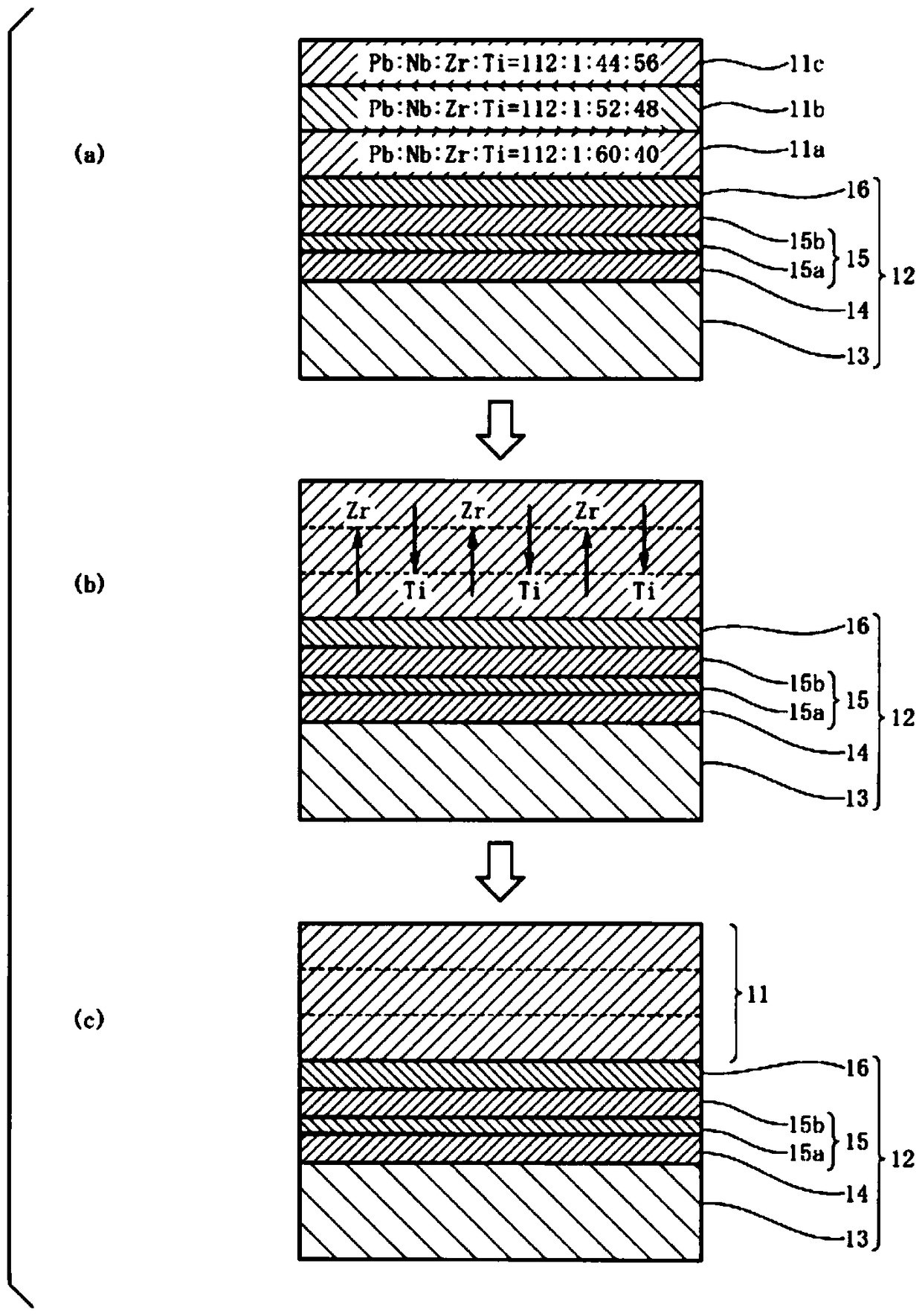
[0044] As the sol-gel solution used to form the PNbZT thin film, prepare a precursor concentration (Pb) with a metal composition ratio of 125 / 10 / 52 / 48 (Pb / Nb / Zr / Ti) and a solvent diluted with 1-butanol. The total of the source, the Nb source, the Zr source, and the Ti source) is a sol-gel solution (E1 solution manufactured by Mitsubishi Materials Corporation) adjusted to 15% by mass in terms of oxide. Here, let the ratio of Nb be higher than the composition formula Pb z Nb x Zr y Ti 1-y O 3 (02 Film and in the SiO 2 TiO x A lower electrode composed of a film and a Pt film, and a crystallization promoting layer is formed on the Pt film.

[0045] In addition, in this Comparative Example 1, and the following Examples 1 to 7 and Comparative Examples 2 to 6, if not particularly limited, a (100)-oriented PZT thin film was formed on the Pt film as a crystallization pro...

Embodiment 2

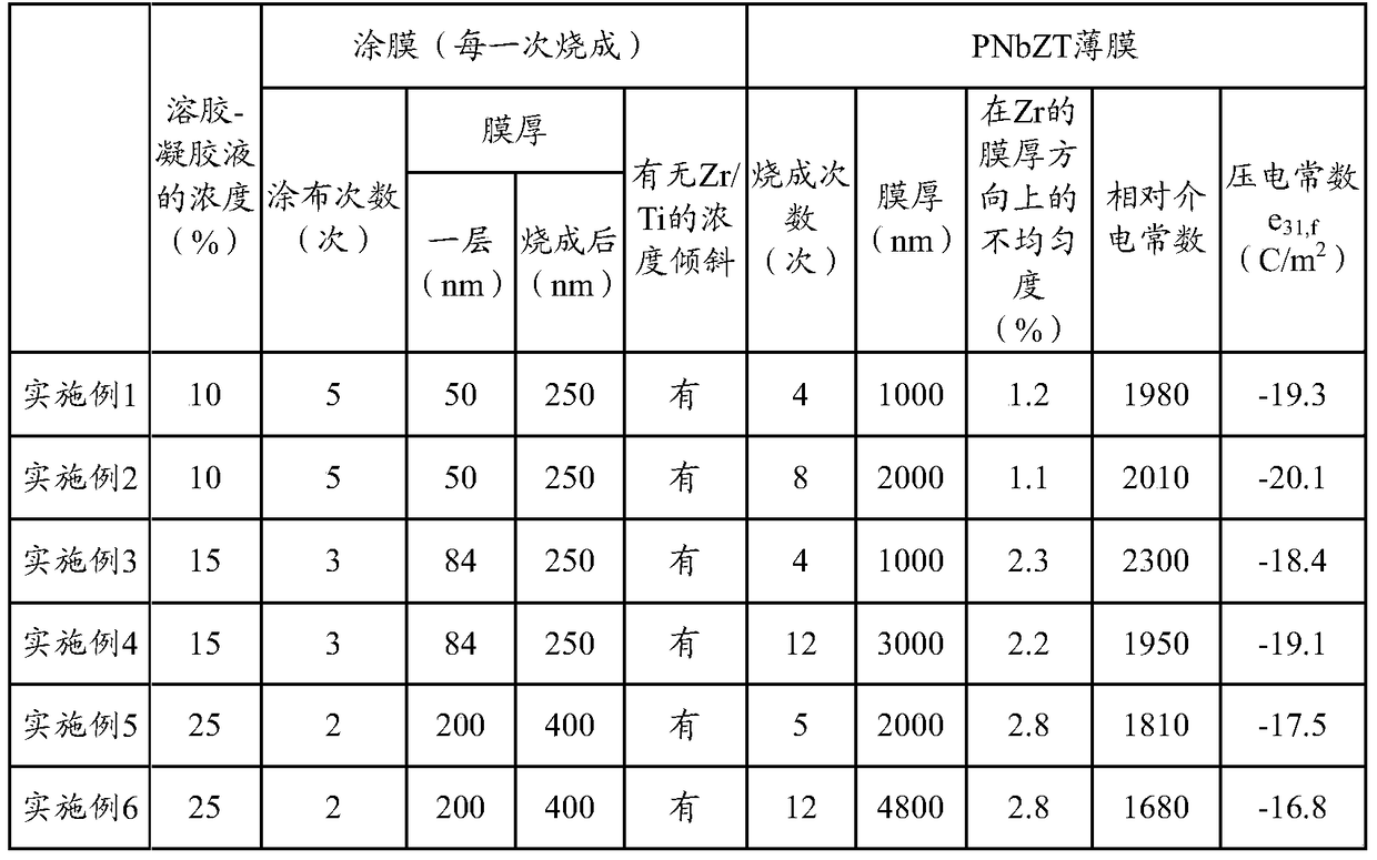
[0054] Except for the step of forming the PNbZT thin film that is fired once and repeated five times from the application of the first to fifth sol-gel solutions to the temporary firing, the total thickness is approximately An eight-layer PNbZT thin film of 2 μm (about 2000 nm) was formed on the crystallization promoting layer of the substrate. In the same manner as in Example 1, the PNbZT thin film was formed on the crystallization promoting layer of the substrate. The substrate on which the PNbZT thin film was formed was used as Example 2.

Embodiment 3、4 and 7

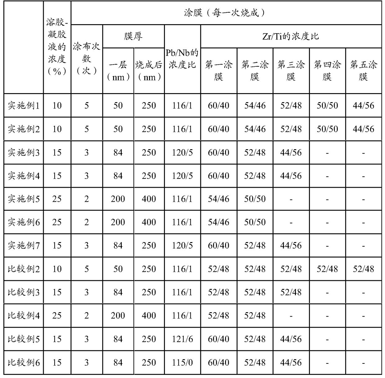
[0056] In addition to the concentration of the sol-gel solution, the number of coatings of the coating film per firing, the film thickness of one layer, the film thickness after firing, the Pt / Nb concentration ratio, and the Zr / Ti per coating film The PNbZT film was formed in the same manner as in Example 1, except that the concentration ratio of PNbZT film, the number of firing of the PNbZT film, and the film thickness of the PNbZT film (hereinafter referred to as various conditions) were changed as described in Tables 1 and 2.

[0057] The substrates on which the PNbZT thin film was formed in this manner were used as Examples 3, 4, and 7.

[0058] In addition, in Examples 3, 4, and 7, only three types of the first to third sol-gel solutions were prepared, and each sol-gel solution was used until the first to third coating films were formed, and then firing was performed. In this regard, in the following examples, in the same manner, a plurality of sol-gel liquids described in Tab...


PUM

PropertyMeasurementUnit
thicknessaaaaaaaaaa
thicknessaaaaaaaaaa
particle diameteraaaaaaaaaa

Abstract

The invention provides a method for manufacturing a PNbZT thin film in which each composition in the film is substantially uniform and has high piezoelectric and dielectric properties. The manufacturing method of the PNbZT film of the present invention comprises the following steps: preparing various sol-gel liquids satisfying the composition formula PbzNbxZryTi1-yO3 and having different zirconium and titanium concentration ratios Zr / Ti, wherein 0<x≤0.05, 0.40 ≤y≤0.60 and 1.05≤z≤1.25; select a specified sol-gel solution from a variety of sol-gel solutions in such a way that the concentration ratio Zr / Ti gradually decreases, and place the sol-gel solution on the substrate The coating and provisional sintering are repeated twice or more, thereby stacking more than two layers of provisional sintering films (11a-11c) whose concentration ratio Zr / Ti gradually becomes smaller on the substrate (12); and multiple provisional sintering A step of obtaining a single PNbZT thin film (11) by firing the films (11a to 11c) together.

Description

Technical field [0001] The present invention relates to a method for manufacturing a PNbZT film used in film piezoelectric devices such as film capacitors. [0002] This application claims priority based on the patent application No. 2013-175100 filed in Japan on August 27, 2013 and the patent application No. 2014-171180 filed in Japan on August 26, 2014, and incorporates the content Used for this. Background technique [0003] It is known that by adding Nb to the Pb formed by the sol-gel method z Zr x Ti 1-x O 3 The PZT film shown to improve the piezoelectric properties (for example: refer to Non-Patent Document 1). In this paper, a research on a PbTiO doped with Nb to grow on a PbTiO prepared by the chemical solution deposition (CSD: Chemical Solution Deposition) method 3 The effect of the (100) orientation PZT film on the seed layer. Specifically, study a Pb with a thickness of 1μm in the (100) orientation 1.1 Zr 0.52 Ti 0.48 O 3 The effect when Nb is doped in the thin film in...

Claims


Application Information

Patent Timeline
Patent Type & Authority Patents(China)
IPC IPC(8): H01L21/316C01G33/00H01L21/8246H01L27/105H01L41/318
CPCH01L28/56H01L28/75H01L21/02197H01L21/02282H10N30/8554H10N30/078
Inventor 土井利浩樱井英章曽山信幸
Owner MITSUBISHI MATERIALS CORP
Why Eureka
Try Eureka