Novel TSV switch board and manufacturing method

An adapter board, a new type of technology, applied in semiconductor/solid-state device manufacturing, electrical components, electric solid-state devices, etc., can solve the problems of thermal expansion coefficient mismatch, high cost, high process technology requirements, etc., and achieve low thermal stress and small parasitic capacitance Effect

Inactive Publication Date: 2016-03-16
苏州含光微纳科技有限公司 +1
View PDF3 Cites 12 Cited by
  • Summary
  • Abstract
  • Description
  • Claims
  • Application Information

AI Technical Summary

Problems solved by technology

However, even with an air-isolated CuTSV design, there is still a thermal expansion coefficient mismatch between the CuTSV

Method used


Image

  • Novel TSV switch board and manufacturing method
  • Novel TSV switch board and manufacturing method
  • Novel TSV switch board and manufacturing method

Examples


Embodiment 1

[0041] A new type of TSV adapter plate structure such as figure 2 Shown:

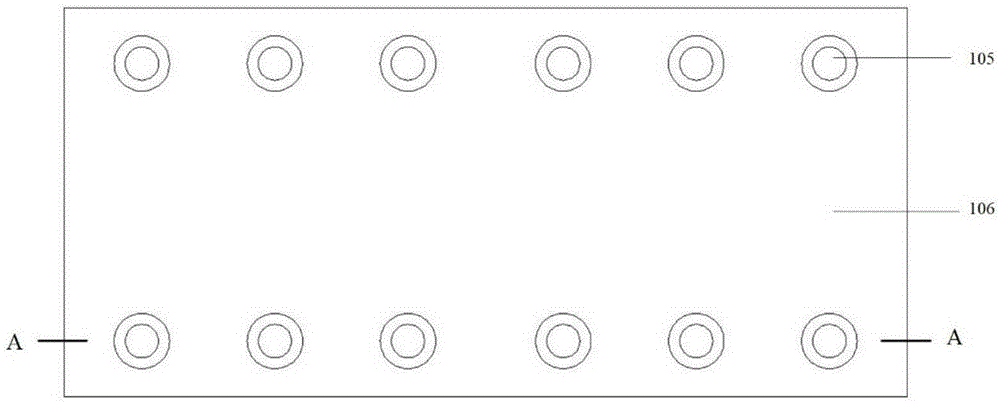
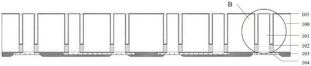
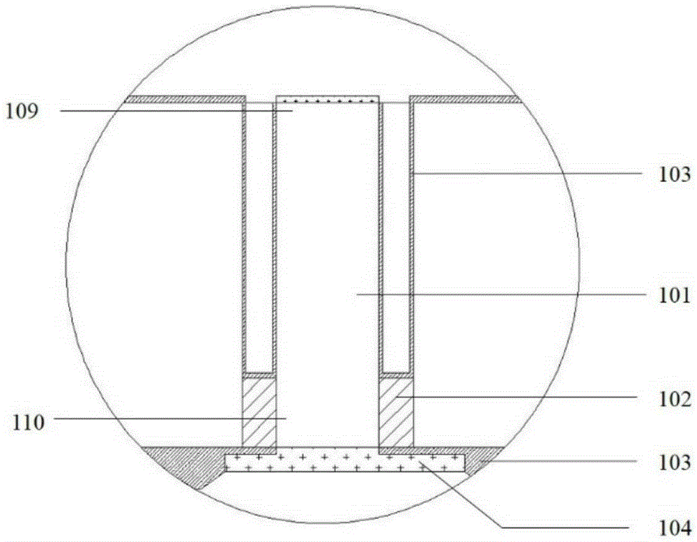
[0042] Substrate 100, there are several free pillars 101 on the said substrate, it is characterized in that one end is separated from the substrate through the gap, the other end is fixed with the substrate through the insulating material 102, and is insulated from the substrate, the upper and lower sides of the substrate 106, 108 ( See figure 1 , Figure 4 ) and the side wall of the free post is covered with a layer of insulating layer 103, and the free end face 105 and the fixed end face 107 of the free post all have ohmic contacts 300 made of metal layers (300 see Figure 11 );

[0043] Preferably, the materials of the substrate and the free column are both low-resistance silicon materials (≤0.1Ω·cm);

[0044] Preferably, the insulating material 102 used for the indirect contact between the free column 101 and the substrate 100 is one of silicon dioxide, glass paste and resin;

[0045] Preferab...

Embodiment 2

[0047] A new type of TSV adapter plate structure such as figure 2 Shown:

[0048] Substrate 100, there are several free pillars 101 on the substrate, it is characterized in that one end is separated from the substrate through a gap, the other end is fixed to the substrate through an insulating material 102, and is insulated from the substrate, the upper and lower sides of the substrate 106, 108 and The side wall of the free post is covered with a layer of insulating layer 103, and the free end face 105 and the fixed end face 107 of the free post all have an ohmic contact 300 made of a metal layer (300 see Figure 11 ).

[0049] Preferably, the materials of the substrate and the free column are both low-resistance silicon materials (≤0.1Ω·cm),

[0050] Preferably, the insulating material 102 used for the indirect contact between the free column 101 and the substrate 100 is one of silicon dioxide, glass paste and resin.

[0051] Preferably, the front and back sides of the su...

Embodiment 3

[0055] A new type of TSV adapter plate structure such as figure 2 Shown:

[0056] Substrate 100, there are several free pillars 101 on the substrate, it is characterized in that one end is separated from the substrate through a gap, the other end is fixed to the substrate through an insulating material 102, and is insulated from the substrate, the upper and lower sides of the substrate 106, 108 and The side wall of the free post is covered with an insulating layer 103, and both the free end face 105 and the fixed end face 107 of the free post have an ohmic contact 300 formed with the metal layer.

[0057] Preferably, the materials of the substrate and the free column are both low-resistance silicon materials (≤0.1Ω·cm),

[0058] Preferably, the insulating material 102 used for the indirect contact between the free column 101 and the substrate 100 is one of silicon dioxide, glass paste and resin.

[0059] Preferably, the front and back sides of the substrate 100 and the side...


PUM


Abstract

The invention relates to a novel TSV switch board and a manufacturing method. The switch board comprises a substrate, the substrate is provided with a plurality of free columns, one ends of the free columns are separated from the substrate via gaps, the other ends of the free columns and the substrate are fixed in an insulation manner via insulating materials, the upper surface and the lower surface of the substrate and sidewalls of the free columns are covered by insulating layers, free end surfaces and fixed end surfaces of the free columns are all provided with ohmic contact formed by metal layers, the substrate is made of a low-resistance silicon material (<=0.1 ohm*cm), the insulating materials employed by indirect contact of the free columns and the substrate refer to one of silicon dioxide, glass frit, and resin, and the metal layers for forming ohmic contact with the free ends and the fixed ends of the free columns refer to one of copper, aluminum, gold, and tin. According to the switch board, the problem of thermal stress caused by mismatch of thermal expansion coefficient between Cu, Au, and W and the silicon substrate is fundamentally avoided, and the TSV switch board with low thermal stress is realized.

Description

technical field [0001] The invention relates to the field of microelectronic packaging, and more specifically relates to a novel TSV adapter board for low-stress packaging and a manufacturing method thereof. Background technique [0002] Through Silicon Via technology (ThroughSiliconVia, TSV) is to make electrical interconnections through silicon wafers through micro-nano processing and other methods. It has the characteristics of small size, high density, and is suitable for building three-dimensional stacked packages. It is a new three-dimensional integrated interconnection solution to transmit delay, reduce noise, improve electrical performance, and reduce power consumption. [0003] In the field of TSV technology, W-TSV, Cu-TSV, Au-TSV, Cu-TSV, etc. are mainly used to realize electrical interconnection. TSV will generate thermal stress due to thermal expansion coefficient mismatch under environmental conditions with large temperature changes, resulting in chip failure. ...

Claims


Application Information

Patent Timeline
IPC IPC(8): H01L23/522H01L21/768
Inventor 马盛林罗荣峰陈兢夏雁鸣任奎丽颜俊
Owner 苏州含光微纳科技有限公司
Why Eureka
Try Eureka