
Ceramic pad array shell structure for inverted installation of hermetic chip

A pad array and airtight technology, which is applied in the field of large-scale integrated circuit ceramic shells, can solve problems such as inability to achieve airtightness, and achieve high mechanical reliability, high precision, and small size

Active Publication Date: 2016-03-23
THE 13TH RES INST OF CHINA ELECTRONICS TECH GRP CORP
View PDF4 Cites 6 Cited by
  • Summary
  • Abstract
  • Description
  • Claims
  • Application Information

AI Technical Summary

Problems solved by technology

[0005] The technical problem to be solved by the present invention is to provide a ceramic pad array housing structure for airtight chip flip-chip mounting, which is used for the packaging of airtight chip flip-chip, and can solve the problem that the existing packaging methods cannot achieve airtightness. problems, can simultaneously have high mechanical reliability, excellent heat dissipation performance and high airtightness

Method used


Image

  • Ceramic pad array shell structure for inverted installation of hermetic chip
  • Ceramic pad array shell structure for inverted installation of hermetic chip
  • Ceramic pad array shell structure for inverted installation of hermetic chip

Examples


Embodiment Construction

[0018] In order to describe the present invention more clearly, the present invention will be further described in detail below in conjunction with the drawings and specific embodiments.

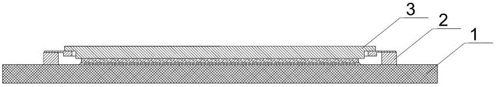
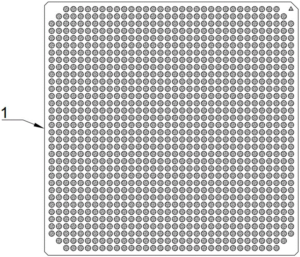
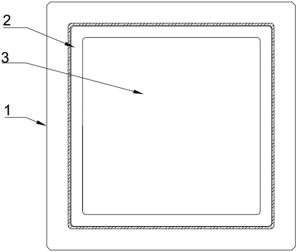
[0019] A ceramic pad array housing structure for airtight chip flip-chip mounting, including a ceramic substrate 1 and a heat dissipation cover 3, where the substrate 1 is arranged with chip flip-chip mounting pads in the form of a grid corresponding to the chip mounting area, for It is connected to the input / output port of the chip, and the other side of the substrate 1 is arranged with ball-planting or column-planting pads as external leads. The ceramic substrate 1 is made of multi-layer alumina ceramic tungsten metallized high-temperature co-fired, and its interior is multi-layered. The layer wiring structure can realize the interconnection between the input / output ports of the chip and the external leads. The middle part of the cover plate 3 is provided with a heat sink for bonding to the...


PUM


Abstract

The invention relates to the technical field of a ceramic shell of a large-scale integrated circuit, in particular relates to a ceramic pad array shell for chip inversion, and particularly discloses a ceramic pad array shell structure for inverted installation of a hermetic chip. A ceramic substrate of multi-layer wiring in the ceramic pad array shell structure is soldered with a metal sealing ring; after the chip is inversely installed, a cooling cover plate is welded with the metal sealing ring by a mode of parallel seam welding to complete package, form hermetic protection for the chip and provide a cooling passage for the chip; and welding pads which are interconnected are respectively arranged at the two sides of the substrate and used for connection of chip input / output (I / O) and external leading. The ceramic pad array shell structure can simultaneously meet requirements of air impermeability and chip cooling, has the advantages of high mechanical reliability, favorable cooling performance and high air impermeability, and can be used for package of the large-scale integrated circuit with a high leading-out end.

Description

technical field [0001] The invention relates to the technical field of large-scale integrated circuit ceramic shells, in particular to a ceramic pad array shell for chip flip-chip. Background technique [0002] The electronic component housing refers to the package of the component, and its main function is to provide electrical (optical) signal interconnection, mechanical protection, environmental protection, and heat dissipation. In the field of high reliability and high performance applications, the ceramic shell based on alumina ceramic material is the preferred packaging form to ensure high air tightness and high reliability. As the scale of integrated circuits, the number of pins, and the degree of integration continue to increase, the pitch of ceramic package pins continues to shrink, and the installation and assembly method gradually develops to surface mount. , The ceramic base of the ceramic column grid array (CCGA) package has become a typical representative of t...

Claims


Application Information

Patent Timeline
Patent Type & Authority Applications(China)
IPC IPC(8): H01L23/10H01L23/373H01L21/52
CPCH01L23/10H01L21/52H01L23/3736
Inventor 张崤君
Owner THE 13TH RES INST OF CHINA ELECTRONICS TECH GRP CORP
Features
  • Generate Ideas
  • Intellectual Property
  • Life Sciences
  • Materials
  • Tech Scout
  • Unparalleled Data Quality
  • Higher Quality Content
  • 60% Fewer Hallucinations
Learn More