Super-junction device and manufacturing method therefor

A technology of super junction devices and manufacturing methods, applied in semiconductor/solid-state device manufacturing, semiconductor devices, electrical components, etc., can solve problems such as circuit damage, loop oscillation, application system current and voltage overshoot, etc., and achieve the minimum increase in capacitance , the effect of increasing the overall capacitance

Active Publication Date: 2016-03-23
SHENZHEN SANRISE TECH CO LTD
View PDF5 Cites 29 Cited by
  • Summary
  • Abstract
  • Description
  • Claims
  • Application Information

AI Technical Summary

Problems solved by technology

[0012] Since dv / dt=igp / Cgd(vd), among them, Vd represents the drain voltage, generally the source is grounded, and Vd is also the source-drain voltage Vds; Cgd(Vd) represents the gate-drain capacitance Cgd is a function of Vd, that is, the value of Cgd The value will change with Vd, igp represents the gate current, and dv / dt represents the change of the drain voltage, that is, Vd; it can be seen that when Vd completely depletes part or all of the N-type column 3 and makes Cgd become very small, at this Under voltage, dv / dt will become very large, which will cause great electromagnetic interference in the circuit or system using the device, affecting the normal operation of the circuit and system; this situation changes from the high-voltage reverse cut-off state to the on-state also exists in the process
This high dv / dt during the switching process, in addition to causing the oscillation of the application circuit, may also cause excessive current and voltage overshoot of the application system, resulting in circuit damage

Method used


Image

  • Super-junction device and manufacturing method therefor
  • Super-junction device and manufacturing method therefor
  • Super-junction device and manufacturing method therefor

Examples


Embodiment 1

[0072] Embodiment 1 of the present invention super junction device:

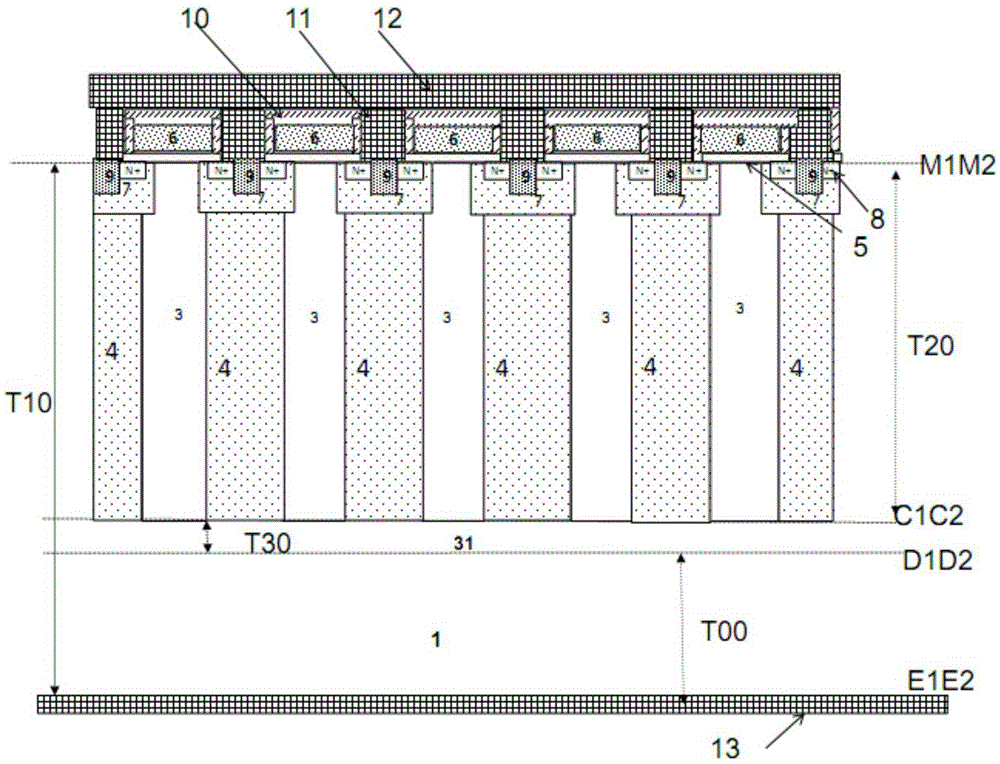
[0073] Such as Figure 5 As shown, it is a cross-sectional view of a super-junction device in an embodiment of the present invention; a super-junction device in an embodiment of the present invention is described by taking a planar gate super-junction N-type MOSFET as an example, and a planar-gate super-junction P-type MOSFET is used to dope the device It can be obtained by replacing the P-type and N-type regions, and the planar gate super-junction P-type MOSFET will not be described in detail.

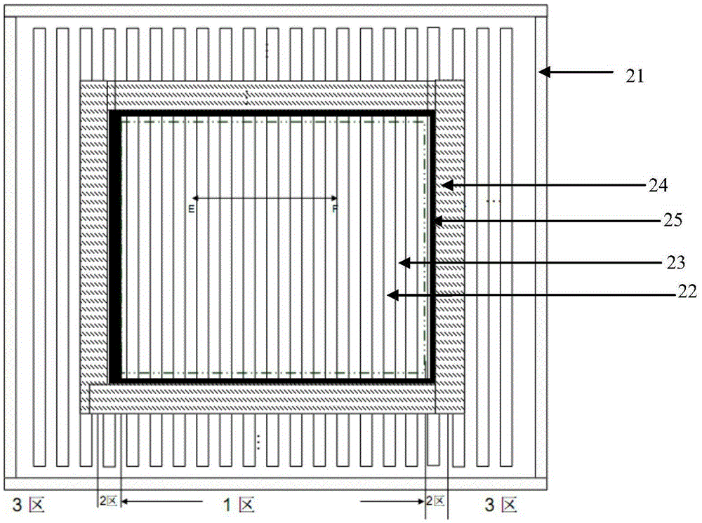
[0074] Such as image 3 As shown, it is a top view of a super junction device according to the embodiment of the present invention Figure 1 A general superjunction structure includes a charge flow region, a terminal region that bears a reverse bias voltage laterally, and a transition region between the charge flow region and the terminal region, and the terminal region surrounds the periphery of the charge flow r...


PUM


Abstract

The invention discloses a super-junction device. A charge flowing region comprises a super-junction structure consisting of a plurality of alternately arranged N-type columns and P-type columns; the N-type columns have two or more widths; backward voltages required for completely exhausting the N-type columns with different widths are different, so that backward voltages corresponding to capacitance minimum values of super-junction units consisting of the N-type columns with different widths are different; and the number of the widths of the N-type columns is set to be two or more, so that the backward voltages corresponding to the capacitance minimum values of the super-junction units are mutually staggered, the super-junction units with the capacitance values greater than the capacitance minimum values always exist under any backward voltage, and the integral capacitance minimum value of the super-junction structure of the charge flowing region is increased and greater than the superposition of the capacitance minimum values of the super-junction units. The invention furthermore discloses a manufacturing method for the super-junction device. According to the super-junction device and the manufacturing method, the capacitance minimum value of the super-junction structure can be increased, the strong voltage change in a switch can be reduced, electromagnetic interference performances of a circuit and a system can be improved, so that the device is easy to use.

Description

technical field [0001] The invention relates to the field of manufacturing semiconductor integrated circuits, in particular to a superjunction device; the invention also relates to a method for manufacturing the superjunction device. Background technique [0002] The super junction structure is composed of alternately arranged N-type pillars and P-type pillars. If the superjunction structure is used to replace the N-type drift region in the vertical double-diffused MOS transistor (VerticalDouble-diffused Metal-Oxide-Semiconductor, VDMOS) device, the conduction path is provided through the N-type column in the conduction state, and the P-type The pillars do not provide a conduction path; in the cut-off state, the PN pillars bear the reverse bias voltage together, forming a super-junction metal-oxide-semiconductor field-effect transistor (Metal-Oxide-Semiconductor Field-Effect Transistor, MOSFET). The super-junction MOSFET can greatly reduce the on-resistance of the device by...

Claims


Application Information

Patent Timeline
Patent Type & Authority Applications(China)
IPC IPC(8): H01L29/06H01L29/78H01L21/336
CPCH01L29/0634H01L29/66477H01L29/78
Inventor 肖胜安曾大杰
Owner SHENZHEN SANRISE TECH CO LTD
Why Eureka
Try Eureka