Silicon gate graphene/black phosphorus transistor and preparation method

A graphene and transistor technology, which is applied in semiconductor/solid-state device manufacturing, semiconductor devices, electrical components, etc., can solve the problems of unfavorable semiconductor device integration and incompatibility, and achieve the effect of guaranteed performance, easy control, and good gate dielectric quality

Inactive Publication Date: 2016-03-23
UNIV OF ELECTRONICS SCI & TECH OF CHINA
View PDF4 Cites 10 Cited by
  • Summary
  • Abstract
  • Description
  • Claims
  • Application Information

AI Technical Summary

Problems solved by technology

The main disadvantage of forming a graphene transistor structure in this way is that it is not compatible with the traditional CMOS process and is not conducive to integration with semiconductor devices. It will encounter greater difficulties when using traditional material deposition methods to fill materials into narrow substrate trenches.

Method used


Image

  • Silicon gate graphene/black phosphorus transistor and preparation method
  • Silicon gate graphene/black phosphorus transistor and preparation method
  • Silicon gate graphene/black phosphorus transistor and preparation method

Examples


Embodiment 1

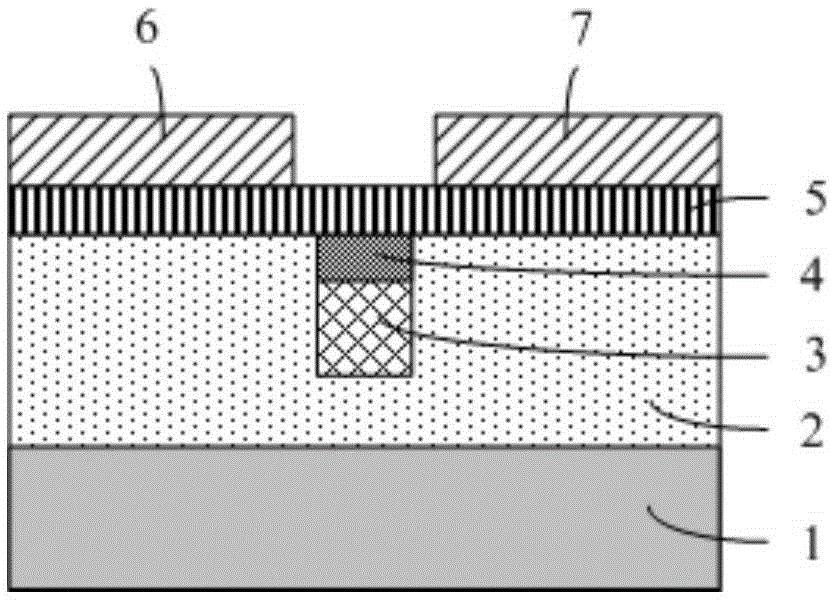
[0039] Embodiment 1: see figure 1 .

[0040] The transistor in this embodiment includes a substrate 1, 2 layers of isolating silicon oxide, 3 gate electrodes of polysilicon, a gate dielectric 4, a source electrode 6, and a drain electrode 7, and the substrate 1 is provided with 2 layers of isolating silicon oxide, and 2 layers of isolating silicon oxide A silicon oxide groove is arranged on the silicon oxide groove, and a polysilicon 3 gate electrode and a gate dielectric 4 are arranged in the silicon oxide groove, 2 layers of isolating silicon oxide and 5 layers of graphene / black phosphorus are arranged on the silicon oxide groove, and 5 layers of graphene / black phosphorus are arranged on the graphene / black phosphorus 5 A source electrode 6 and a drain electrode 7 are arranged above the layer. The gate electrode is polysilicon 3, and the gate dielectric 4 is silicon oxide.

Embodiment 2

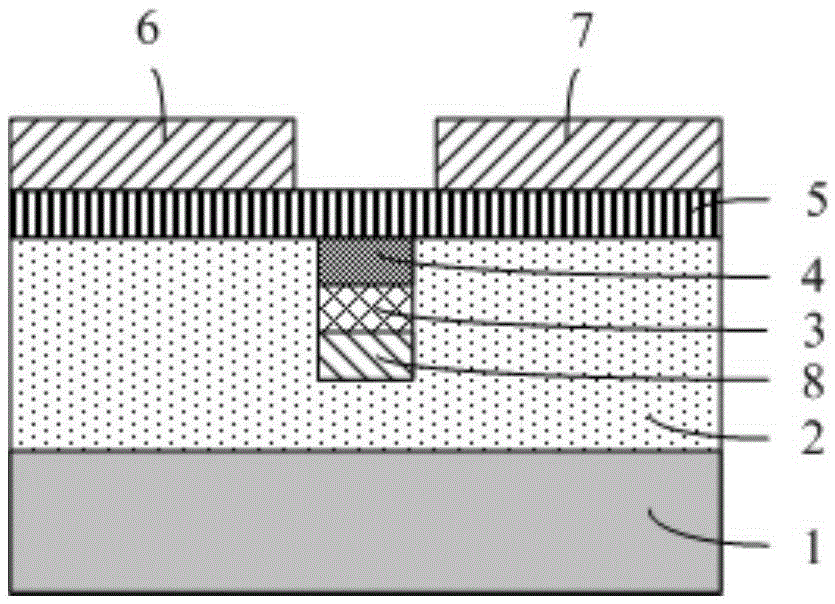
[0041] Example 2: see figure 2 .

[0042] The difference between this embodiment and Embodiment 1 is that the gate electrode of this embodiment is an overlapping combination of refractory metal 8 and polysilicon 3 , refractory metal 8 is at the bottom of the silicon oxide tank, and polysilicon 3 is above the refractory metal.

Embodiment 3

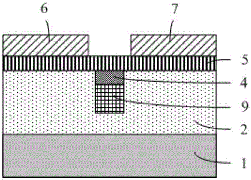
[0043] Embodiment 3: see image 3 .

[0044] The difference between this embodiment and Embodiment 1 is that the gate electrode of this embodiment is a refractory metal silicide 9 .


PUM


Abstract

The present invention discloses a silicon gate graphene/black phosphorus transistor and a preparation method, and relates to a semiconductor device technology. The transistor disclosed by the present invention comprises a substrate, a gate electrode, a gate dielectric, a source electrode and a drain electrode, and is characterized in that: a silicon oxide isolation layer is arranged on the substrate, a silicon oxide groove is disposed on the silicon oxide isolation layer, the gate electrode and the gate dielectric are disposed inside the silicon oxide groove, a graphene/black phosphorus layer is disposed on the surface of the substrate, and the source electrode and the drain electrode are disposed above the graphene/black phosphorus layer. The silicon gate graphene/black phosphorus transistor and the preparation method have the advantages that: 1, the method is easy to control, is good in process repeatability, and is compatible with a conventional semiconductor silicon process; 2, high gate dielectric quality is easily obtained; 3, filling of a relatively narrow groove is easy to achieve; 4, application potential of large scale integration is realized; and 5, performance of a graphene/black phosphorus film is ensured to the maximum extent.

Description

technical field [0001] The present invention relates to semiconductor device technology. Background technique [0002] Since the development of silicon integrated circuit technology, trillions of dollars in equipment and technology investment around the world have made integrated circuit technology a very strong industrial capability. At the same time, long-term scientific research investment has enabled people to have a very deep and thorough understanding of the various properties of silicon and its derivatives, making it the most of more than 100 elements in nature. This is a very valuable accumulation of knowledge. [0003] In recent years, technologies such as 4th generation mobile communication, mobile communication mobile phones, high-speed wireless Internet, Bluetooth, and satellite TV services using MPGE standard to realize wireless video and image transmission have surged, and wireless communication technology has developed by leaps and bounds. The huge demand of ...

Claims


Application Information

Patent Timeline
Patent Type & Authority Applications(China)
IPC IPC(8): H01L29/78H01L21/34H01L29/423H01L21/44
CPCH01L29/78H01L29/401H01L29/4236H01L29/42364H01L29/66969
Inventor 李平王刚张庆伟陈远富
Owner UNIV OF ELECTRONICS SCI & TECH OF CHINA
Why Eureka
Try Eureka