Semiconductor device and forming method thereof

A semiconductor and device technology, applied in the field of semiconductor manufacturing, can solve the problems of lateral double diffusion field effect transistor (LDMOS transistor performance needs to be improved, etc.), and achieve the effect of reducing gate-drain parasitic capacitance

Active Publication Date: 2016-03-30
SEMICON MFG INT (SHANGHAI) CORP
View PDF4 Cites 14 Cited by
  • Summary
  • Abstract
  • Description
  • Claims
  • Application Information

AI Technical Summary

Problems solved by technology

[0004] However, the performance of the existing lateral double diffused field effect transistor (LDMOS transistor) still needs to be improved.

Method used


Image

  • Semiconductor device and forming method thereof
  • Semiconductor device and forming method thereof
  • Semiconductor device and forming method thereof

Examples


Embodiment Construction

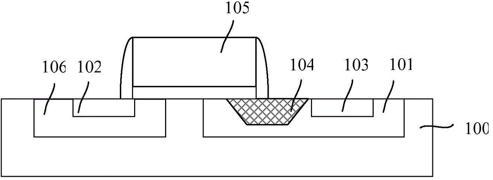
[0032] The performance of the existing LDMOS transistors still needs to be further improved. The parasitic capacitance of the gate and drain of the LDMOS transistor is the main parameter affecting the switching rate of the LDMOS transistor. Especially when the LDMOS transistor is used as a high-frequency switching device, the parasitic capacitance of the gate and drain of the LDMOS transistor The effect of switching rate is particularly prominent.

[0033] Research has found that the gate-drain parasitic capacitance of LDMOS transistors is related to parameters such as the area facing the gate electrode and the drift region, the distance between the gate electrode and the drift region, and the dielectric constant of the gate dielectric layer. The smaller the gate-drain parasitic capacitance, the better the switch The smaller the influence of the rate, usually by increasing the facing area of ​​the gate electrode and the drift region, increasing the thickness of the gate dielect...


PUM


Abstract

A semiconductor device and a forming method thereof are provided. The semiconductor device comprises a semiconductor substrate, a first shallow trench isolation structure which is disposed in the semiconductor substrate and of which the top surface is higher than the surface of the semiconductor substrate, a drift region which is disposed in the semiconductor substrate and surrounds the first shallow trench isolation structure and of which the depth is greater than the depth of the first shallow trench isolation structure, a first body region which is disposed in the semiconductor substrate on one side of the drift region and is of a doping type opposite to the doping type of the drift region, a first gate structure which is disposed on the semiconductor substrate and stretches across and covers part of the surfaces of the body region, the semiconductor substrate, the drift region and the first shallow trench isolation structure, a first drain region which is disposed in the drift region on one side of the first gate structure, and a first source region which is disposed in the first body region on the other side of the first gate structure. The gate-drain parasitic capacitance of the semiconductor device is reduced.

Description

technical field [0001] The invention relates to the field of semiconductor manufacturing, in particular to a semiconductor device and a forming method thereof. Background technique [0002] The power field effect transistor mainly includes two types: a vertical double-diffused field effect transistor (VDMOS, Vertical Double-Diffused MOSFET) and a lateral double-diffused field effect transistor (LDMOS, Lateral Double-Diffused MOSFET). Among them, compared with the vertical double diffused field effect transistor (VDMOS), the lateral double diffused field effect transistor (LDMOS) has many advantages, for example, the latter has better thermal stability and frequency stability, higher gain and durability stability, lower feedback capacitance and thermal resistance, as well as constant input impedance and simpler bias current circuitry. [0003] In the prior art, a conventional N-type lateral double-diffused field effect transistor (LDMOS transistor) structure is as follows f...

Claims


Application Information

Patent Timeline
Patent Type & Authority Applications(China)
IPC IPC(8): H01L21/336H01L29/78H01L29/06
Inventor 程勇洪中山
Owner SEMICON MFG INT (SHANGHAI) CORP
Why Eureka
Try Eureka