

Semiconductor device and manufacturing method for reducing surface topology and character line stringer residual
A manufacturing method and word line technology, applied to the structure of semiconductor devices and the field of forming such semiconductor devices
- Summary
- Abstract
- Description
- Claims
- Application Information
AI Technical Summary
Problems solved by technology
Method used
Image

Examples
Embodiment Construction
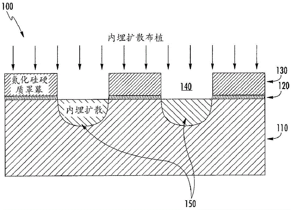
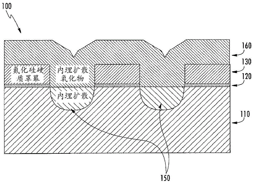
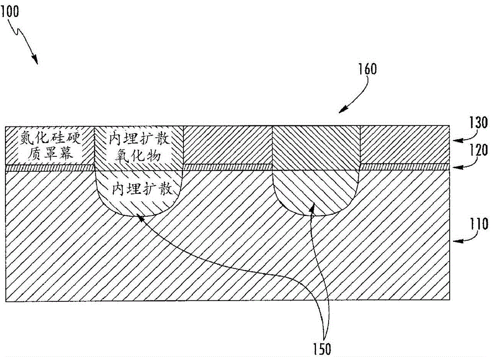
[0063] In order to further explain the technical means and effects of the present invention to achieve the intended purpose of the invention, below in conjunction with the accompanying drawings and preferred embodiments, the semiconductor device proposed according to the present invention and the reduction of surface relief and character line stringer residues The specific implementation, structure, method, steps, features and effects of the manufacturing method are described in detail below.
[0064] The aforementioned and other technical contents, features and effects of the present invention will be clearly presented in the following detailed description of preferred embodiments with reference to the drawings. For the convenience of description, in the following embodiments, the same elements are denoted by the same numbers.
[0065] Non-volatile memory refers to semiconductor devices that can store data even if the electrical supply is removed from the memory. Non-volatil...
PUM
 Abstract
Description
Claims
Application Information