Wavelength-allocation-based three-dimensional optical on-chip network router communication system and method

An optical on-chip network and wavelength allocation technology, applied in the field of communications, which can solve the problems of high delay and limited network scalability.

Active Publication Date: 2016-03-30
XIDIAN UNIV
View PDF3 Cites 9 Cited by
  • Summary
  • Abstract
  • Description
  • Claims
  • Application Information

AI Technical Summary

Problems solved by technology

[0004] The purpose of the present invention is to address the defects in the above-mentioned prior art, provide a three-dimensional optical on-chip network router communication system and method based on wavelength allocation, and solve the problems of limited network scalability and high time delay caused by using a single wavelength communication

Method used


Image

  • Wavelength-allocation-based three-dimensional optical on-chip network router communication system and method
  • Wavelength-allocation-based three-dimensional optical on-chip network router communication system and method
  • Wavelength-allocation-based three-dimensional optical on-chip network router communication system and method

Examples


Embodiment Construction

[0037] The present invention will be described in further detail below in conjunction with the accompanying drawings.

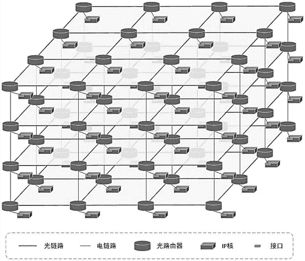
[0038] The three-dimensional optical on-chip network router communication system based on wavelength distribution of the present invention includes an optical transmission network and an electrical control network, and the scale of use is k N 2 3DMesh topology, where k and N are positive even numbers. The 3D optical on-chip network has a total of k layers, and each layer has N 2 nodes. The nodes in the layer are connected through waveguides, and the nodes between layers are connected through TSVs and TSPVs. Each node in the optical transmission network includes a modulator, a demodulator, and an optical router, wherein the injection / exit port of the router is connected with the optical transmission network through an optical / electrical interface. The electrical control network and the optical transmission network adopt the same topology, where each IP core...


PUM


Abstract

The invention relates to a wavelength-allocation-based three-dimensional optical on-chip network router communication system and method. The communication system employs a photoelectric mixing type 3D mesh network topological structure and a novel seven-port clog-free optical router capable of realizing multi-wavelength communication; and when the system is applied to a three-dimensional optical on-chip network, no wavelength conversion is needed. Because of utilization of the optical router, the consumed number of optical devices like micro ring resonators and waveguides and the like is reduced. Besides, according to the communication method, when a node of each layer sends out an optical signal, the employed wavelengths are identical; and optical signals with all wavelengths can be received at all layers, so that problems of severe network congestion, low link utilization rate, and limited expansibility due to utilization of single wavelength communication by the existing optical on-chip network architecture can be solved. Therefore, with the system and method, the network congestion probability can be reduced; the communication delay can be reduced; and the throughput capacity and network saturation point can be improved.

Description

technical field [0001] The invention belongs to the field of communication, and in particular relates to a three-dimensional optical on-chip network router communication system and method based on wavelength distribution, which solves the problem of severe blockage of the existing 3DMesh optical on-chip network using a single wavelength communication network, and improves communication efficiency. Background technique [0002] With the advancement of integrated circuit manufacturing technology, on-chip networks appear, which apply computer network ideas to chip design and use networks to replace the original global wiring. The network on chip constructs the global wiring, so the electrical characteristics are optimized and easy to control. Multiple communication flows share wiring resources to make full use of resources: when a node is idle, other nodes can continue to use network resources. With the further shrinking of the size of integrated circuits and the rapid increas...

Claims


Application Information

Patent Timeline
Patent Type & Authority Applications(China)
IPC IPC(8): H04Q11/00H04L12/801H04L12/933
CPCH04L47/10H04L49/109H04Q11/0005H04Q11/0062H04Q2011/0032H04Q2011/0075
Inventor 顾华玺朱可馨杨银堂王琨谭伟张博文
Owner XIDIAN UNIV
Why Eureka
Try Eureka