Touch screen, manufacturing method for touch screen, and touch apparatus

A production method and touch screen technology, which are applied in touch devices, touch screens and their production fields, can solve problems such as troublesome operation and tolerance, and achieve the effects of saving costs, small tolerances, and avoiding the introduction of tolerances

Active Publication Date: 2016-04-06
深圳市合力泰光电有限公司
View PDF5 Cites 2 Cited by
  • Summary
  • Abstract
  • Description
  • Claims
  • Application Information

AI Technical Summary

Problems solved by technology

The process is cumbersome to operate and easily introduces tolerances

Method used


Image

  • Touch screen, manufacturing method for touch screen, and touch apparatus
  • Touch screen, manufacturing method for touch screen, and touch apparatus
  • Touch screen, manufacturing method for touch screen, and touch apparatus

Examples


Embodiment 1

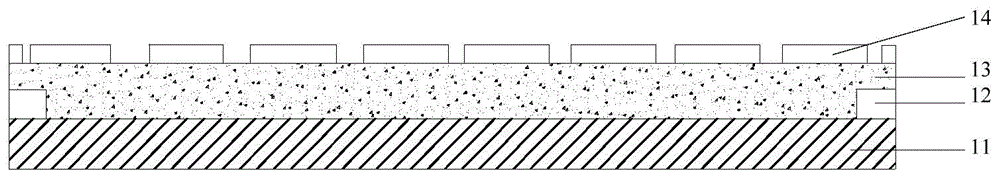
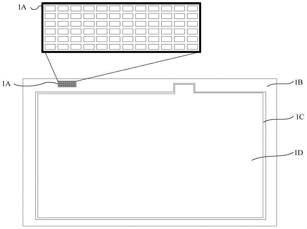
[0025] Set the touch screen that this embodiment makes is the touch screen of the full ITO product G1M structure of black, and its structure can refer to figure 1 and figure 2 . For a better understanding of the public, the inventors in figure 2 A partial enlargement of the depicted object is also drawn in . Such as figure 1 As shown, the touch screen includes a transparent substrate 11 , a decoration layer 12 , an anti-reflection film layer 13 , a transparent electrode layer 14 , and a flexible circuit board (not shown) on the transparent electrode layer 14 . Such as figure 2 As shown: 1A is the antenna area, 1B is the non-functional area, 1C is the isolated area, and 1D is the functional area.

[0026] (1) The transparent substrate 11 is provided. Choose strengthened silicate glass, the strengthening depth is about 8um. It is required that the spectral transmittance of the transparent substrate 11 at the wavelength position of 550 nm is greater than 91%. The trans...

Embodiment 2

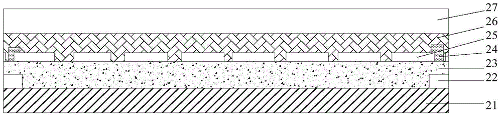
[0033] Set the touch screen that this embodiment makes is the black G1F structure, and its structure can refer to image 3 and Figure 4 . For a better understanding of the public, the inventors in Figure 4 A partial enlargement of the depicted object is also drawn in . Such as image 3 As shown, the touch screen includes a transparent substrate 21, a decorative layer 22, an antireflection film layer 23, a transparent electrode layer 24, a silver paste conductive layer 25, an optically transparent adhesive layer 26, a thin film sensor 26, and a silver paste conductive layer 25 and a thin film A flexible circuit board (not shown in the figure) is placed between the sensors 26 . Such as Figure 4 As shown: 2A is the antenna area, 2B is the non-functional area, 2C is the ground line area in the silver paste conductive layer, 2D is the isolation area, and 2E is the functional area.

[0034] (1) The transparent substrate 21 is provided. Choose strengthened silicate glass, t...


PUM


Abstract

The invention discloses a touch screen. The touch screen comprises a transparent electrode layer made of a transparent conductive material, wherein an antenna region of the transparent electrode layer comprises a plurality of mutually isolated small regions; a non antenna region of the transparent electrode layer comprises a functional region and a non-functional region which are isolated from each other; and the transparent conductive material in the non-functional region is connected with a ground wire. According to the touch screen provided by an embodiment of the invention, the antenna region of the transparent electrode layer is high in independence; the non antenna region is good in electrostatic resistance; and the touch screen has the advantages of simple structure, low manufacturing cost, uniform thickness, small tolerance and the like. The invention furthermore discloses a manufacturing method for the touch screen and a touch apparatus.

Description

technical field [0001] The invention belongs to the technical field of touch devices, and in particular relates to a touch screen, a manufacturing method thereof, and a touch device. Background technique [0002] In the process of manufacturing touch screens with G1M (glass-one-multi, glass single-layer multi-point) structure and G1F (glass-one-film, glass sensor plus thin film sensor) structure by the existing small chip technology, laser dry etching technology is used to make When touching the glass sensor of the screen, it is necessary to remove the unnecessary transparent conductive material on the edge with etching paste or acid-resistant ink. This process is cumbersome to operate and is prone to introducing tolerances. Contents of the invention [0003] The present invention aims to solve one of the technical problems in the related art at least to a certain extent. Therefore, the first object of the present invention is to provide a simple and easy-to-use touch sc...

Claims


Application Information

Patent Timeline
Patent Type & Authority Applications(China)
IPC IPC(8): G06F3/041
Inventor 万娅鹏陈学刚何再钱
Owner 深圳市合力泰光电有限公司
Why Eureka
Try Eureka