An Addressable Imaging Detection Chip for Local Wavefront Measurement

A local wave and imaging technology, applied in the field of imaging detection, can solve the problem of unable to initialize, verify or continuously update the wavefront sequence, and difficult to carry out real-time wavefront data measurement, calculation, wavefront construction, and occupancy. A large number of electronic resources and other issues have been achieved to achieve the effects of high wavefront measurement accuracy, good adaptability, and high mapping efficiency

Active Publication Date: 2018-12-14
HUAZHONG UNIV OF SCI & TECH
View PDF8 Cites 0 Cited by
  • Summary
  • Abstract
  • Description
  • Claims
  • Application Information

AI Technical Summary

Problems solved by technology

[0003] So far, the adaptive optical imaging scheme based on wavefront measurement and adjustment still has some defects in the imaging detection of complex targets and environments, mainly in the following aspects: In terms of detection, it is only suitable for the space environment and the light wave field with relatively clean, stable, slow-changing or small instantaneous field of view; Concentrate on the spatial region where only local wavefront measurement and adjustment needs to be performed; (3) Based on the acquired image information, it is usually possible to identify the abnormal image liquid crystal micro-optical block including its rough orientation, but it is difficult to perform local wavefront measurement and adjustment through the conventional wavefront measurement and adjustment architecture Accurate measurement and adjustment of the wavefront corresponding to the abnormal imaging liquid crystal micro-optical block; (4) It is impossible to quickly implement the wavefront spatial variation inspection to initialize, verify or continuously update the wavefront sequence, and to find the abnormal local wavefront area and predict the orientation, Disturbance category or changing dynamic potential; (5) The global wavefront measurement and adjustment of the instantaneous field of view requires a large amount of electronic resources. In the case of limited random electronic resource allocation, it is difficult to carry out real-time wavefront data measurement for fast moving targets or transient physical and chemical processes. , solution and wavefront construction

Method used


Image

  • An Addressable Imaging Detection Chip for Local Wavefront Measurement
  • An Addressable Imaging Detection Chip for Local Wavefront Measurement
  • An Addressable Imaging Detection Chip for Local Wavefront Measurement

Examples


Embodiment Construction

[0031] In order to make the object, technical solution and advantages of the present invention clearer, the present invention will be further described in detail below in conjunction with the accompanying drawings and embodiments. It should be understood that the specific embodiments described here are only used to explain the present invention, not to limit the present invention. In addition, the technical features involved in the various embodiments of the present invention described below can be combined with each other as long as they do not constitute a conflict with each other.

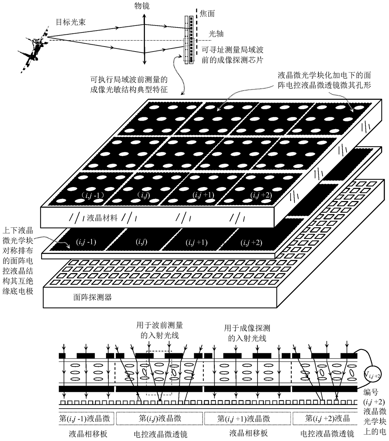
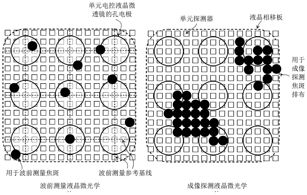
[0032] figure 1 It is a structural schematic diagram of an imaging detection chip that can address and measure local wavefronts according to an embodiment of the present invention. An addressable imaging detection chip for measuring a local wavefront according to an embodiment of the present invention includes: an addressable local wavefront measurement and adjustment and imaging detection stru...


PUM


Abstract

The invention discloses an imaging detection chip capable of addressably measuring local wavefront. The imaging detection chip comprises an addressable power-up liquid crystal micro-optical structure, an area array visible light detector and a drive and control preprocessing module. The liquid crystal micro-optical structure is divided into a plurality of liquid crystal micro-optical blocks capable of independently applying electrical drive and control signals. The liquid crystal micro-optical blocks have the same surface shape and structure size; the powered-up liquid crystal micro-optical block is a liquid crystal microlens array block, and the rest non-powered-up liquid crystal micro-optical blocks are liquid crystal phase shift blocks; and the liquid crystal micro-optical structure divided into the liquid crystal micro-optical blocks divides the area array visible light detector corresponding thereto into area array visible light detector blocks having the same shape and scale, and each area array visible light detector block comprises detectors in same quantity and arrangement mode. The imaging detection chip has an imaging detection effect of executing addressable selection and changing local wavefront measurement, is convenient to use and is easy to be coupled with a conventional imaging optical system.

Description

technical field [0001] The invention belongs to the technical field of imaging detection, and more specifically relates to an imaging detection chip capable of addressing and measuring local wavefronts. Background technique [0002] In the solar-terrestrial or deep space environment, the light waves emitted or stimulated from the earth, the sun, stars, disturbances or even deceptive light sources constitute the background light field on which the target depends. By reflecting / refracting / scattering sunlight, moonlight, starlight or artificial light, the object embeds its own structure and shape information into the fluctuating light field and transports it to the imaging detection structure, and realizes electronic image data generation through photoelectric conversion. Generally speaking, the optical wave field that transports the image information of the target exhibits a specific shape wave front and its moving sequence in the background and artificial optical environment,...

Claims


Application Information

Patent Timeline
Patent Type & Authority Patents(China)
IPC IPC(8): G01J9/00
CPCG01J9/00
Inventor 张新宇雷宇信钊炜魏冬桑红石王海卫谢长生
Owner HUAZHONG UNIV OF SCI & TECH
Why Eureka
Try Eureka