Nano composite stacked phase-change film and preparation method and application thereof
A nano-composite and thin-film technology, applied in the field of microelectronics, can solve the problems that the thermal stability of the thin film is not very high and the thermal stability needs to be improved, and achieve the effects of improving thermal stability, high thermal stability and improving signal-to-noise ratio.
- Summary
- Abstract
- Description
- Claims
- Application Information
AI Technical Summary
Problems solved by technology
Method used
Image

Examples
Embodiment 1
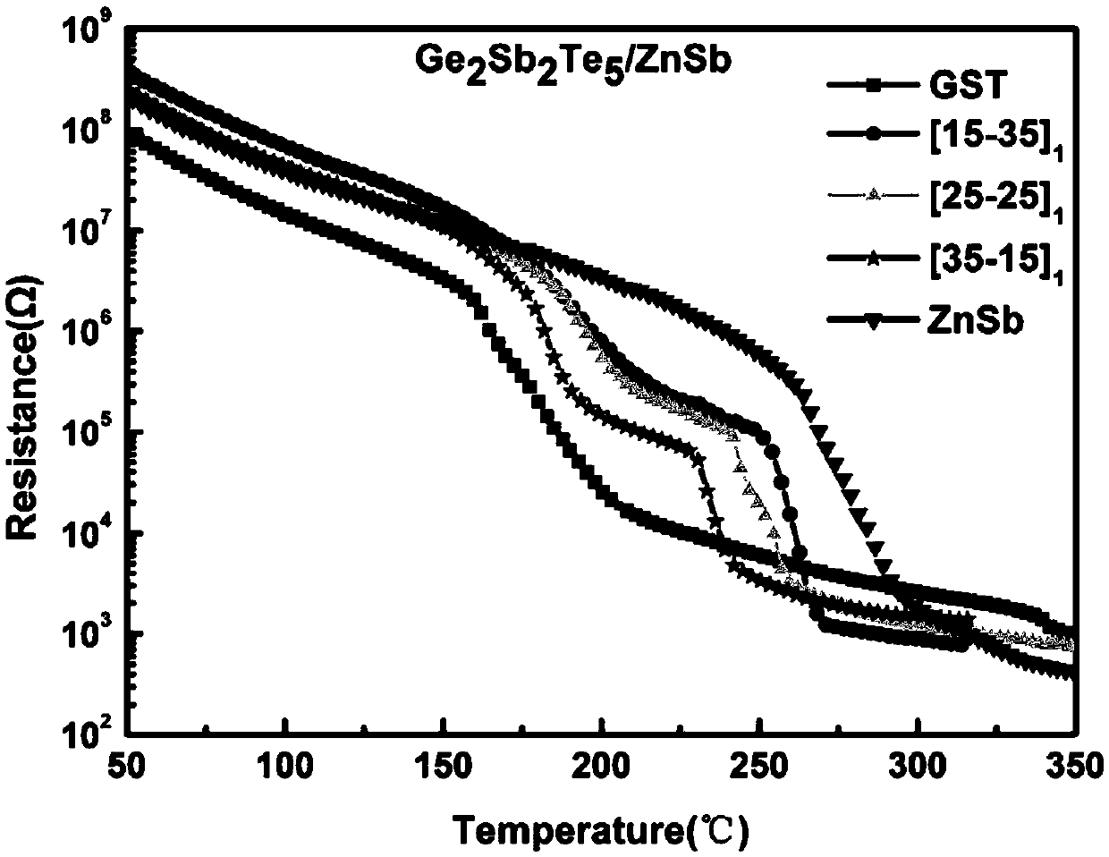
[0032] Ge prepared in this example 2 Sb 2 Te 5 / ZnSb nanocomposite stacked phase change film with a total thickness of 50nm and a general structural formula of [Ge 2 Sb 2 Te 5 (a) / ZnSb(b)]x, the specific structure is [Ge 2 Sb 2 Te 5 (15nm) / ZnSb(35nm)] 1 、[Ge 2 Sb 2 Te 5 (25nm) / ZnSb(25nm)] 1 、[Ge 2 Sb 2 Te 5 (35nm) / ZnSb(15nm)] 1 .
[0033] 1. Clean SiO2 2 / / Si(100) substrate surface and back, remove dust particles, organic and inorganic impurities:
[0034] (a) Place the substrate in an ethanol solution, and clean it ultrasonically for 15 minutes to remove dust particles and inorganic impurities on the surface of the substrate;
[0035] (b) The substrate is placed in an acetone solution, and ultrasonically cleaned for 15 minutes to remove organic impurities on the surface of the substrate;
[0036] (c) Place the substrate in deionized water, clean it ultrasonically for 15 minutes, and clean the surface again;
[0037] (d) Take out the substrate, dry it with ...
Embodiment 2
[0079] Nanocomposite stacked phase-change films made of Ge 2 Sb 2 Te 5 Thin films and ZnSb thin films are arranged alternately to form stacked thin film units, Ge 2 Sb 2 Te 5 The thickness of the thin film is 25nm, the thickness of the ZnSb thin film is 25nm, and they are alternately arranged to form a layer structure of stacked thin film units, and the thickness of the unit is 50nm.
[0080] The preparation method of the nanocomposite stacked phase change film adopts the following steps:
[0081] (1) cleaning SiO2 2 / Si(100) substrate surface and back, remove dust particles, organic and inorganic impurities;
[0082] (2) Install the sputtering target, set the RF power, gas flow and sputtering pressure;
[0083] (3) Prepare Ge by room temperature magnetron sputtering method 2 Sb 2 Te 5 / ZnSb nanocomposite stacked phase change film, specifically adopt the following steps:
[0084] (3-1) Rotate the substrate to Ge 2 Sb 2 Te 5 Target, open Ge 2 Sb 2 Te 5 RF power s...
Embodiment 3
[0088] Nanocomposite stacked phase-change films made of Ge 2 Sb 2 Te 5 Thin films and ZnSb thin films are arranged alternately to form stacked thin film units, Ge 2 Sb 2 Te 5 The thickness of the thin film is 35nm, and the thickness of the ZnSb thin film is 35nm, which are alternately arranged to form a stacked thin film unit as a layer structure. The thickness of the stacked thin film unit is 50 nm.
[0089] The preparation method of the nanocomposite stacked phase change film adopts the following steps:
[0090] (1) cleaning SiO2 2 / Si(100) substrate surface and back, remove dust particles, organic and inorganic impurities;
[0091] (2) Install the sputtering target, set the RF power, gas flow and sputtering pressure;
[0092] (3) Prepare Ge by room temperature magnetron sputtering method 2 Sb 2 Te 5 / ZnSb nanocomposite stacked phase change film, specifically adopt the following steps:
[0093] (3-1) Rotate the substrate to Ge 2 Sb 2 Te 5 Target, open Ge 2 Sb...
PUM
| Property | Measurement | Unit |
|---|---|---|
| Thickness | aaaaa | aaaaa |
| Thickness | aaaaa | aaaaa |
| Thickness | aaaaa | aaaaa |
Abstract
Description
Claims
Application Information
PatSnap Eureka turns technology decisions into work you can execute. Powered by our Innovation Knowledge Graph, it runs expert workflows across engineering, life sciences, materials and intellectual property. Get your review-ready output in minutes.


