Unidirectional magnetization semiconductor waveguide integration multiple-mode interference magneto-optical isolator

A waveguide integration and multi-mode interference technology, applied in the field of integrated optics, can solve the problems of semiconductor integration, difficulty in preparation, and difficulty in magnetic field integration or packaging, and achieve simplified magnetic field application methods, easy preparation and packaging, and low insertion loss Effect

Active Publication Date: 2016-05-04
UNIV OF ELECTRONIC SCI & TECH OF CHINA
View PDF3 Cites 11 Cited by
  • Summary
  • Abstract
  • Description
  • Claims
  • Application Information

AI Technical Summary

Problems solved by technology

The problems of the proposed MMI magneto-optical isolator are mainly (1) The device structure is based on the epitaxial magneto-optic thin film material on the GGG substrate, which cannot realize semiconductor integration.
(2) The propos

Method used


Image

  • Unidirectional magnetization semiconductor waveguide integration multiple-mode interference magneto-optical isolator
  • Unidirectional magnetization semiconductor waveguide integration multiple-mode interference magneto-optical isolator
  • Unidirectional magnetization semiconductor waveguide integration multiple-mode interference magneto-optical isolator

Examples


Embodiment Construction

[0025] Practical example 1

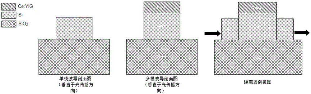
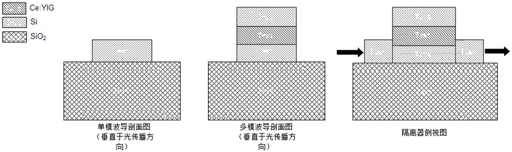
[0026] Such as figure 1 As shown, this structure adopts SOI substrate as the low refractive index layer, and grows magneto-optical thin film layer, low refractive index layer and semiconductor waveguide layer on it to form the device. The low refractive index layer of the single-mode waveguide is SiO 2 , the thickness is 2um, the semiconductor waveguide layer is silicon, the width is 500nm, the thickness is 350nm, and the uppermost low refractive index layer is made of air. In a single-mode waveguide, the propagation of light is limited to one transmission mode, the fundamental mode TM00 of the TM mode and the fundamental mode TE00 of the TE mode.

[0027] The second part of the isolator is the first multimode waveguide, the waveguide structure is from bottom to top and the thickness of each layer is SiO 2 (2um) / Si(500nm) / CeYIG(300nm) / air, the waveguide width is 500nm, it supports TM00 mode and TM01 mode. Since the TM00 mode is mainly distribut...


PUM

PropertyMeasurementUnit
Thicknessaaaaaaaaaa
Thicknessaaaaaaaaaa
Thicknessaaaaaaaaaa

Abstract

The invention belongs to the field of integrated optics, and particularly relates to a unidirectional magnetization semiconductor waveguide integration multiple-mode interference magneto-optical isolator. The isolator is composed of a single-mode waveguide unit, a multi-mode waveguide unit and a single-mode waveguide unit which are connected in sequence, and optical waves are transmitted through the waveguide units. An SIO substrate is adopted as a base layer for all waveguides of the waveguide units of the isolator. Each waveguide unit is composed of at least one corresponding waveguide. In the multi-mode waveguide unit, the first multi-mode waveguide sequentially comprises a low refractive index layer, a magneto-optical thin film layer, a semiconductor waveguide thin film layer and a low refractive index layer from top to bottom; the second multi-mode waveguide sequentially comprises a low refractive index layer, a semiconductor waveguide thin film layer, a magneto-optical thin film layer, a semiconductor waveguide thin film structural layer and a low refractive index layer from top to bottom. Modes are longitudinally distributed by enabling the width of multi-mode interference waveguides to be consistent to that of single-mode waveguides. The MMI optical isolator structure under unidirectional magnetization is achieved, the magnetic field application method is simplified, and therefore the device is easy to prepare and package.

Description

technical field [0001] The invention belongs to the field of integrated optics, in particular to a unidirectional magnetization semiconductor waveguide integrated multimode interference magneto-optical isolator. Background technique [0002] With the increasing demand for transmission bandwidth in communication network systems, optical communication and optical interconnection technologies are gradually developing towards high integration, high bandwidth, and low energy consumption. In order to improve the system transmission bandwidth and data stability, backscattering and reflection in the optical path have become an important problem that must be solved. The backward transmitted light generated by various reasons will adversely affect the stable operation of optical components such as light sources and amplifiers. As a result, a non-reciprocal passive device that only allows light to transmit forward along the optical path - an optical isolator. [0003] Optical isolato...

Claims


Application Information

Patent Timeline
IPC IPC(8): G02B6/27
CPCG02B6/2746
Inventor 毕磊税科弋邓龙江
Owner UNIV OF ELECTRONIC SCI & TECH OF CHINA
Why Eureka
Try Eureka