Fabrication method for test element group (TEG) test key on a thin film transistor (TFT) array substrate

A technology of an array substrate and a manufacturing method, which is applied in the field of manufacturing TEG test keys on a TFT array substrate, can solve the problems of large photoresist pattern area and difficulty in removing the photoresist, so as to achieve increased area, easy photoresist stripping process, and The effect of reducing the area

Active Publication Date: 2016-05-04
WUHAN CHINA STAR OPTOELECTRONICS TECH CO LTD
View PDF3 Cites 7 Cited by
  • Summary
  • Abstract
  • Description
  • Claims
  • Application Information

AI Technical Summary

Problems solved by technology

In addition, there are also a few manufacturers that use the Clear mode to form the photoresist pattern, then the formed photoresist pattern will basically cover the entire substrate, only exposing the first active layer 210 and the second active layer 210 that need to be exposed for subsequent ion implantation. The two ends of the active layer 220, obviously, in this mode, the area of ​​the photoresist pattern is too large, and it is difficult to remove the photoresist in the subsequent photoresist stripping process.

Method used


Image

  • Fabrication method for test element group (TEG) test key on a thin film transistor (TFT) array substrate
  • Fabrication method for test element group (TEG) test key on a thin film transistor (TFT) array substrate
  • Fabrication method for test element group (TEG) test key on a thin film transistor (TFT) array substrate

Examples


Embodiment Construction

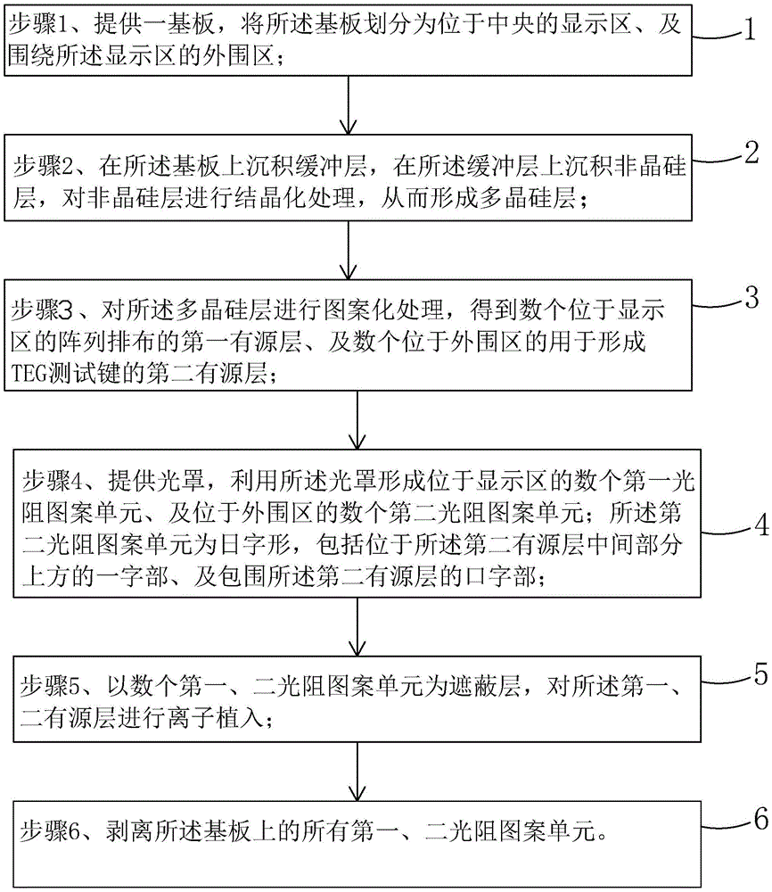
[0037] In order to further illustrate the technical means adopted by the present invention and its effects, the following describes in detail in conjunction with preferred embodiments of the present invention and accompanying drawings.

[0038] see figure 2, the manufacture method of TEG test key on a kind of TFT array substrate provided by the invention, comprises the following steps:

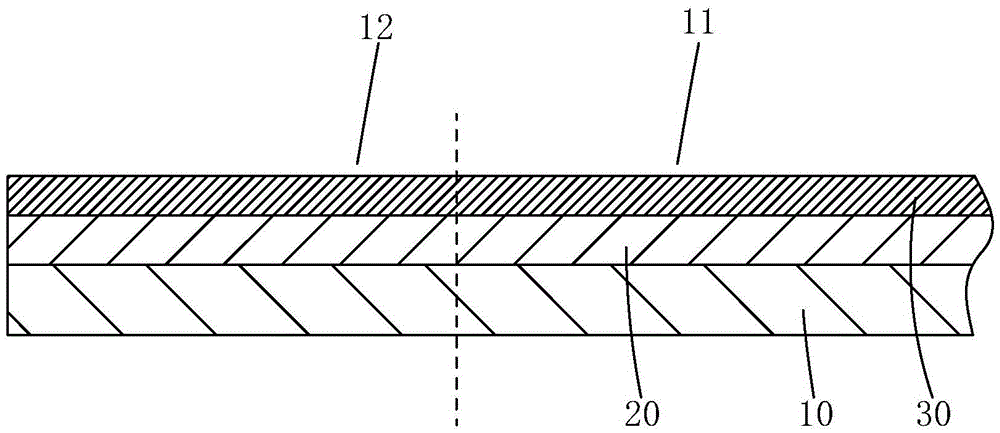
[0039] Step 1. Provide a substrate 10 , and divide the substrate 10 into a central display area 11 and a peripheral area 12 surrounding the display area 11 .

[0040] Preferably, the substrate 10 is a glass substrate.

[0041] Step 2, such as image 3 As shown, a buffer layer 20 is deposited on the substrate 10 , an amorphous silicon layer is deposited on the buffer layer 20 , and the amorphous silicon layer is crystallized to form a polysilicon layer 30 .

[0042] Specifically, the amorphous silicon layer is crystallized through a rapid thermal annealing process.

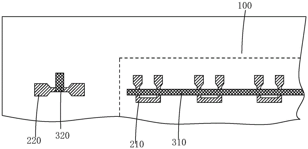
[0043] Step 3, if Fi...


PUM


Abstract

The invention provides a fabrication method for a test element group (TEG) test key on a thin film transistor (TFT) array substrate. The fabrication method comprises the following steps of forming a plurality of first active layers arranged on a display region and a plurality of second active layers arranged on a peripheral region and used for forming the TEG test key on a substrate; and forming a plurality of first photoresist pattern units and a plurality of second photoresist pattern units by using a particularly-designed optical cover, wherein the second photoresist pattern units are in stud link shapes and comprise straight line parts arranged above the middle parts of the second active layers and latticed parts encircling the second active layers. Compared with a conventional optical cover adopting a Dark mode, the area of the photoresist pattern in an ion implantation range of the active layer for defining and forming the TEG test key is expanded, and thus, the too small photoresist area is prevented to cause the problem of difficulty in photoresist removal due to serious coking of a load effect during the subsequent ion implantation process; moreover, compared with a traditional optical cover adopting Clear mode, the area of the photoresist pattern on the whole substrate is reduced, and thus, the subsequent photoresist stripping process is easy to proceed.

Description

technical field [0001] The invention relates to the field of display technology, in particular to a method for manufacturing a TEG test key on a TFT array substrate. Background technique [0002] Thin Film Transistor (ThinFilmTransistor, TFT) is the main driving element in the current Liquid Crystal Display (Liquid Crystal Display, LCD) and active matrix driven organic electroluminescent display (ActiveMatrixOrganicLight-EmittingDiode, AMOLED), directly related to the display performance of the flat panel display . Thin film transistors have various structures, and there are also various materials for preparing thin film transistors with corresponding structures, among which low temperature polysilicon (Low Temperature Poly-silicon, LTPS) material is a more preferred one. [0003] Both LCD and AMOLED include a TFT array substrate. Generally, in the product manufacturing stage of the display panel, in order to monitor the characteristic value of the effective light-emitting...

Claims


Application Information

Patent Timeline
Patent Type & Authority Applications(China)
IPC IPC(8): H01L21/77H01L21/027G03F7/20G03F7/00
CPCG03F7/00G03F7/20H01L21/027H01L21/77H01L2021/775
Inventor 张嘉伟张占东刘元甫赵瑜陈辰
Owner WUHAN CHINA STAR OPTOELECTRONICS TECH CO LTD
Why Eureka
Try Eureka