High-avalanche capability power semiconductor transistor structure and preparation method thereof

A technology for power semiconductors and avalanche tolerance, which is applied in semiconductor/solid-state device manufacturing, semiconductor devices, electrical components, etc., and can solve problems such as increased fluctuations in process preparation, increased device manufacturing costs, and poor breakdown uniformity. Eliminate the impact of process fluctuations on devices, reduce production costs, and improve avalanche tolerance

Inactive Publication Date: 2016-05-04
SOUTHEAST UNIV
View PDF3 Cites 2 Cited by
  • Summary
  • Abstract
  • Description
  • Claims
  • Application Information

AI Technical Summary

Problems solved by technology

[0004] In order to improve the avalanche tolerance of the device, the current common practice is to increase the device’s ability to pass a large current by increasing the area of ​​the device, but the manufacturing cost of the device increases; or change the doping concentration of the region related to the avalanche tolerance of the device , this can theoretically improve the avalanche tolerance, but after the doping concentration increases, the fluctuation of the process preparation will increase, and some P-type impurity concentration peaks will be generated at the bottom of the P-type body region, which will easily lead to the deterioration of the breakdown uniformity. Reduced avalanche tolerance and reduced yield

Method used


Image

  • High-avalanche capability power semiconductor transistor structure and preparation method thereof
  • High-avalanche capability power semiconductor transistor structure and preparation method thereof
  • High-avalanche capability power semiconductor transistor structure and preparation method thereof

Examples


Embodiment 1

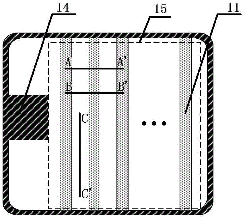
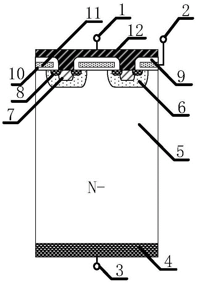
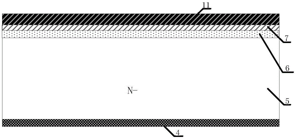
[0035] A power semiconductor transistor structure with high avalanche tolerance, comprising an N-type substrate 4 serving as a drain region, an N-type epitaxial layer 5 is arranged on the N-type substrate 4, and a P-type epitaxial layer 5 is arranged on the surface of the N-type epitaxial layer 5. The strip-shaped body region 6, the surface of the P-type strip-shaped body region 6 is provided with a heavily doped N-type source region 8 and a heavily doped P-type source region 7, and an insulating gate oxide layer 10 is arranged on the N-type epitaxial layer 5. Conductive polysilicon 11 is provided on the insulating gate oxide layer 10, except for the heavily doped P-type body region 7 and part of the heavily doped N-type source region 8, the conductive polysilicon 11 exists above the surface of the N-type epitaxial layer 5, so An insulating dielectric layer 9 is provided on the conductive polysilicon 11, and a source metal 12 is connected to the heavily doped P-type body region...

Embodiment 2

[0040] A method for preparing a power semiconductor transistor structure with high avalanche resistance according to claim 1, characterized in that:

[0041] The first step: first select heavily doped N-type silicon material as the N-type substrate 4, and epitaxially grow the N-type epitaxial layer 5, the thickness of the N-type epitaxial layer 5 is about 50 μm, and the resistivity is about 13ohm*cm - 3 ~18ohm*cm - 3 ;

[0042] Step 2: Deposit photoresist on the N-type epitaxial layer 5 and etch, then ion-implant boron, the implantation dose is about 1×10 13 cm - 3 ~1×10 14 cm - 3 , and high-temperature (above 1000° C.) annealing to form multiple P-type bow body regions 13;

[0043] Step 3: Thermally oxidize on the N-type epitaxial layer 5 to form an insulating gate oxide layer 10, then deposit conductive polysilicon 11 on the silicon dioxide, then deposit photoresist and etch away a part of the conductive polysilicon and silicon dioxide, through self-aligned ion imp...


PUM


Abstract

The invention provides a high-avalanche capability power semiconductor transistor structure, which comprises an N-type substrate used as a drain region, wherein an N-type epitaxial layer is arranged on the N-type substrate; P-type strip body regions are arranged on the surface of the N-type epitaxial layer; a heavily doped N-type source region and a heavily doped P-type source region are arranged on the surface of each P-type strip body region; an insulated gate oxidation layer is arranged on the N-type epitaxial layer; conductive polysilicon is arranged on the insulated gate oxidation layer, and is located at the upper part of the region between the adjacent P-type strip body regions and two sides of the conductive polysilicon respectively cover the adjacent P-type strip body regions; an insulated medium layer is arranged on the conductive polysilicon; the heavily doped N-type source regions and the heavily doped N-type source regions are connected with a source metal; the high-avalanche capability power semiconductor transistor structure is characterized in that the P-type strip body regions extend towards the N-type epitaxial layer to form a plurality of P-type arched body regions; and the P-type arched body regions are evenly distributed on the P-type strip body regions and are embedded into the N-type epitaxial layer. According to the high-avalanche capability power semiconductor transistor structure, a preparation method of a traditional power semiconductor transistor is reserved; the avalanche capability is improved; the chip area is reduced; and the cost is relatively low.

Description

technical field [0001] The invention mainly relates to the technical field of power semiconductor devices, in particular to a power semiconductor transistor with high avalanche tolerance and a preparation method thereof, especially suitable for electric vehicles, motor speed regulation, inverters, uninterruptible power supplies, electronic switches, high-fidelity audio, automobiles Electrical and electronic rectifiers. Background technique [0002] The vertical double-diffused metal-oxide semiconductor field-effect transistor has the advantages of both bipolar transistors and ordinary metal-oxide semiconductor field-effect transistor devices. It is an ideal power device for both switching applications and linear applications, because it has nearly infinite Large static input impedance characteristics, very fast switching time, positive temperature coefficient of on-resistance, approximately constant transconductance, extremely fast voltage reversal speed and other characteri...

Claims


Application Information

Patent Timeline
Patent Type & Authority Applications(China)
IPC IPC(8): H01L29/06H01L29/78H01L21/336
CPCH01L29/0603H01L29/0611H01L29/0688H01L29/66477H01L29/78
Inventor 孙伟锋周锦程杨卓祝靖陆生礼时龙兴
Owner SOUTHEAST UNIV
Why Eureka
Try Eureka