Circuit simulation method for fin edge roughness effect in fin type field effect transistor

A field effect transistor and circuit simulation technology, applied in electrical digital data processing, special data processing applications, instruments, etc., can solve problems such as unpredictability, wrong estimation of circuit fluctuations, and inability to take into account changes in device fluctuations.

Active Publication Date: 2016-05-11
PEKING UNIV
View PDF5 Cites 2 Cited by
  • Summary
  • Abstract
  • Description
  • Claims
  • Application Information

AI Technical Summary

Problems solved by technology

However, this method has many limitations
First of all, this method is not predictive at all, that is, it cannot take into account fluctuations caused by device design parameters or process changes
Secondly, this method completely regard...

Method used


Image

  • Circuit simulation method for fin edge roughness effect in fin type field effect transistor
  • Circuit simulation method for fin edge roughness effect in fin type field effect transistor
  • Circuit simulation method for fin edge roughness effect in fin type field effect transistor

Examples


Embodiment Construction

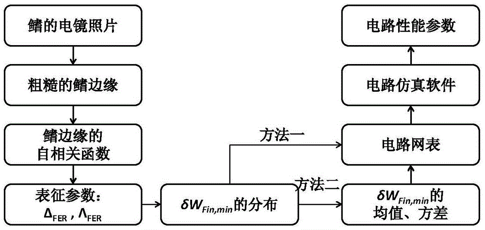
[0027] The circuit simulation method for the roughness of the fin edge in the fin field effect transistor provided by the present invention will be described in detail below by way of examples and in conjunction with the accompanying drawings.

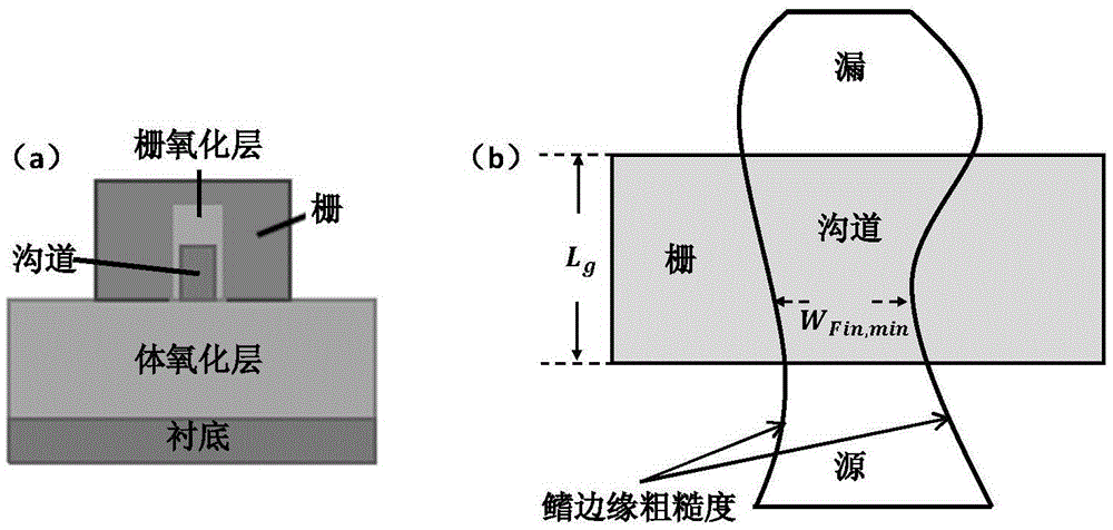
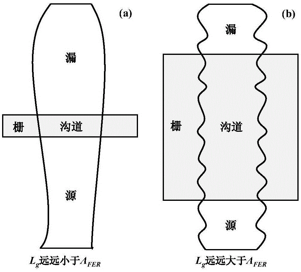
[0028] This example considers the influence of fin edge roughness on the performance parameter of static random access memory (SRAM) circuit - static noise margin (SNM) in dual-gate fin field effect transistor based on SOI substrate. The overall process is as follows figure 1 shown. The basic structure and parameters of the double-gate fin field effect transistor are defined as figure 2 shown. Among them, L g much smaller than Λ FER and L g much larger than Λ FER The schematic diagrams of fin edge roughness in these two extreme cases are shown in image 3 shown.

[0029] Specific steps:

[0030] 1) if Figure 4 As shown, according to the electron microscope photo of the grid, the rough grid edge is extracted, its autocorrelat...


PUM


Abstract

The invention discloses a circuit simulation method for a fin edge roughness effect in a fin type field effect transistor, and belongs to the field of a microelectronic device. The circuit simulation method is based on a predictable intensive model; a rough fin edge is extracted from an electron microscopy image of a fin line; the self-correlation function of the fin edge is calculated; then fin width distribution under the influence of the fin edge roughness can be obtained by a computational formula; and the fin width distribution is embedded into a simulation netlist of circuit simulation software to perform circuit simulation to obtain circuit performance parameters caused by the fin edge roughness. By adoption of the circuit simulation method, the device characteristic fluctuation influences can be accurately obtained; all the parameters can be subjected to reference regulation by a result obtained by TCAD monte carlo simulation; and compared with the conventional method, the fluctuation of a (sub-threshold slope) SS of the device, and the correlation between the fluctuation of the SS and a threshold voltage Vth can be predicted.

Description

technical field [0001] The invention belongs to the field of microelectronic devices, and relates to a circuit simulation method for fin edge roughness in a fin field effect transistor. Background technique [0002] With the gradual reduction of the scale of semiconductor devices, the influence of random fluctuations in the devices is becoming more and more difficult to ignore. The random fluctuation of the device is caused by the inevitable process uncertainty in the device manufacturing process, which will lead to the fluctuation of the electrical characteristics of the device, such as the threshold voltage, and further, it will inevitably cause the fluctuation of the circuit performance parameters. Fluctuations in circuit performance parameters will eventually lead to yield loss during chip fabrication. Therefore, circuit designers need to take into account the impact of random fluctuations in devices on circuit characteristics in advance when designing circuits, which r...

Claims


Application Information

Patent Timeline
IPC IPC(8): G06F17/50
CPCG06F30/367
Inventor 黄如蒋晓波王润声
Owner PEKING UNIV
Why Eureka
Try Eureka