Transformer shielding layer design method for flyback switching power supply

A switching power supply and design method technology, applied in the manufacture of inductors/transformers/magnets, preventing/reducing unwanted electric/magnetic influences, circuits, etc., can solve power supply products that are difficult to meet EMC standards, electronic load interference, EMI, etc. problem, to achieve the effect of common mode noise suppression, increase product cost, and low cost

Active Publication Date: 2016-05-25
ZHEJIANG UNIV
View PDF6 Cites 9 Cited by
  • Summary
  • Abstract
  • Description
  • Claims
  • Application Information

AI Technical Summary

Problems solved by technology

With the switching characteristics of switching devices getting better and better, high dv/dt and di/dt bring serious EMI problems
On the one hand, these serious EMI problems will make it difficult for power supply products to meet the relevant EMC standards. On the other hand, even if the relevant EMC standards are met, common-mode noise will sometimes form on the sensitive load side, causing serious interference to electronic loads.
In theory, fixing the width, thickn

Method used


Image

  • Transformer shielding layer design method for flyback switching power supply
  • Transformer shielding layer design method for flyback switching power supply
  • Transformer shielding layer design method for flyback switching power supply

Examples


Embodiment Construction

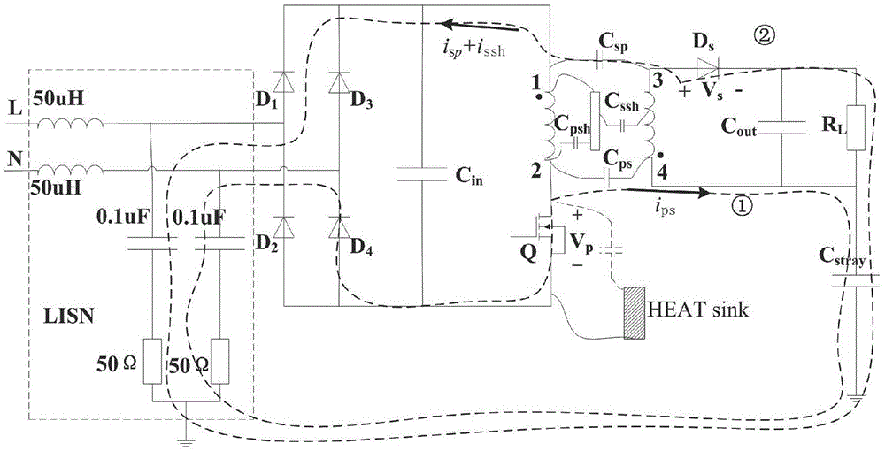
[0038] In order to describe the present invention more specifically, the technical solutions of the present invention will be described in detail below in conjunction with the accompanying drawings and specific embodiments.

[0039] The transformer shielding layer design method of the flyback switching power supply of the present invention uses finite element analysis software to simulate the structural capacitance between the original and secondary windings and the structural capacitance between the secondary winding and the shielding layer under different shielding layer widths, and then Use the common-mode current evaluation formula to calculate the shielding layer width when the common-mode current is minimum, including the following steps:

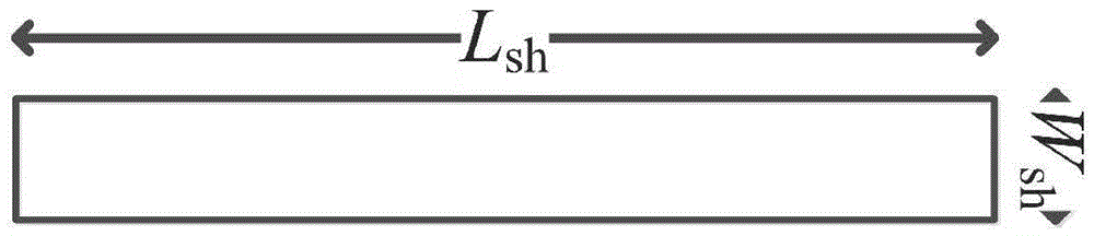
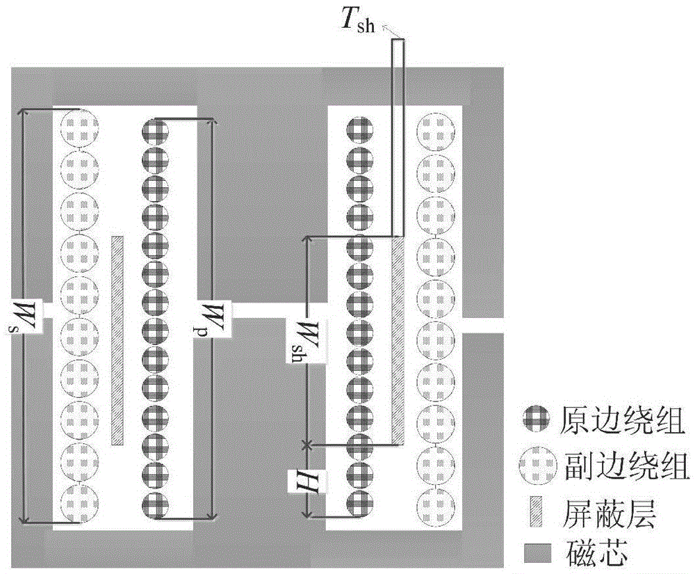
[0040] (1) Measure and estimate the structural dimensions such as the winding diameter, copper foil layer thickness, and winding spacing of the transformer.

[0041] The structural capacitance between the transformer winding and the s...


PUM


Abstract

The invention discloses a transformer shielding layer design method for a flyback switching power supply. The transformer shielding layer design method comprises the steps of 1) measuring and estimating structures and electrical parameters of a transformer; 2) setting a shielding layer length as the circumference of the layer, setting the thickness according to actual supply, wherein the position of the layer is set based on a proper value; obtaining structural capacitance between a primary side winding and a secondary side winding of the transformer, and structural capacitance between the secondary side winding and a shielding copper foil layer under different shielding layer widths in a simulation manner through finite element software analysis; 3) calculating common-mode evaluation equivalent capacitance in the transformer under the different shielding layer widths, and drawing a common-mode equivalent capacitance-shielding layer width characteristic curve; and 4) obtaining the shielding layer width when the common-mode evaluation equivalent capacitance is equal to 0 according to the drawn characteristic curve, wherein the obtained shielding layer width is the optimal shielding layer width for restraining common-mode current of the transformer. Compared with the existing common-mode restraining technology, the transformer shielding layer design method has the advantages of simple realization, low cost, capability of reducing the volume and the weight of the common-mode filter, obvious restraining effect, and the like.

Description

technical field [0001] The invention belongs to the technical field of transformer design, and in particular relates to a design method for a transformer shielding layer of a flyback switching power supply. Background technique [0002] Flyback switching power supplies are widely used in communications, service systems and low-power electronic equipment due to their isolation function. These devices all need to meet relevant electromagnetic compatibility (EMC) standards, so there are often certain electromagnetic interference (EMI) filtering measures in the design of switching power supply products. With the switching characteristics of switching devices getting better and better, high dv / dt and di / dt bring serious EMI problems. On the one hand, these serious EMI problems will make it difficult for power supply products to meet the relevant EMC standards. On the other hand, even if the relevant EMC standards are met, common-mode noise will sometimes form on the sensitive lo...

Claims


Application Information

Patent Timeline
IPC IPC(8): H01F41/00H01F27/36
CPCH01F27/36H01F41/00
Inventor 陈恒林肖记
Owner ZHEJIANG UNIV
Why Eureka
Try Eureka