Manufacturing method for fine circuit

A production method and technology of fine lines, which are applied in the manufacture of printed circuits, printed circuits, electrical components, etc., can solve the problems of large pool effect, affect the accuracy of lines, increase the amount of side erosion, etc., to accelerate the exchange, improve the exchange speed, The effect of improving accuracy

Inactive Publication Date: 2016-05-25
JIANGMEN SUNTAK CIRCUIT TECH
View PDF4 Cites 2 Cited by
  • Summary
  • Abstract
  • Description
  • Claims
  • Application Information

AI Technical Summary

Problems solved by technology

[0004] The present invention aims at the problem that in the production process of the existing PCB, when the outer layer is etched, the pool effect is large, which increases the amount of side erosion, thereby affecting the accuracy of the circuit, and provides a fine circuit that can reduce the amount of side erosion and improve the accuracy of the circuit. Production Method

Method used


Image

  • Manufacturing method for fine circuit
  • Manufacturing method for fine circuit

Examples


Embodiment

[0020] This embodiment provides a method for manufacturing a fine circuit, which can reduce the pool effect during etching of the outer layer and improve the etching capability.

[0021] The specific production steps are as follows:

[0022] (1) multilayer board

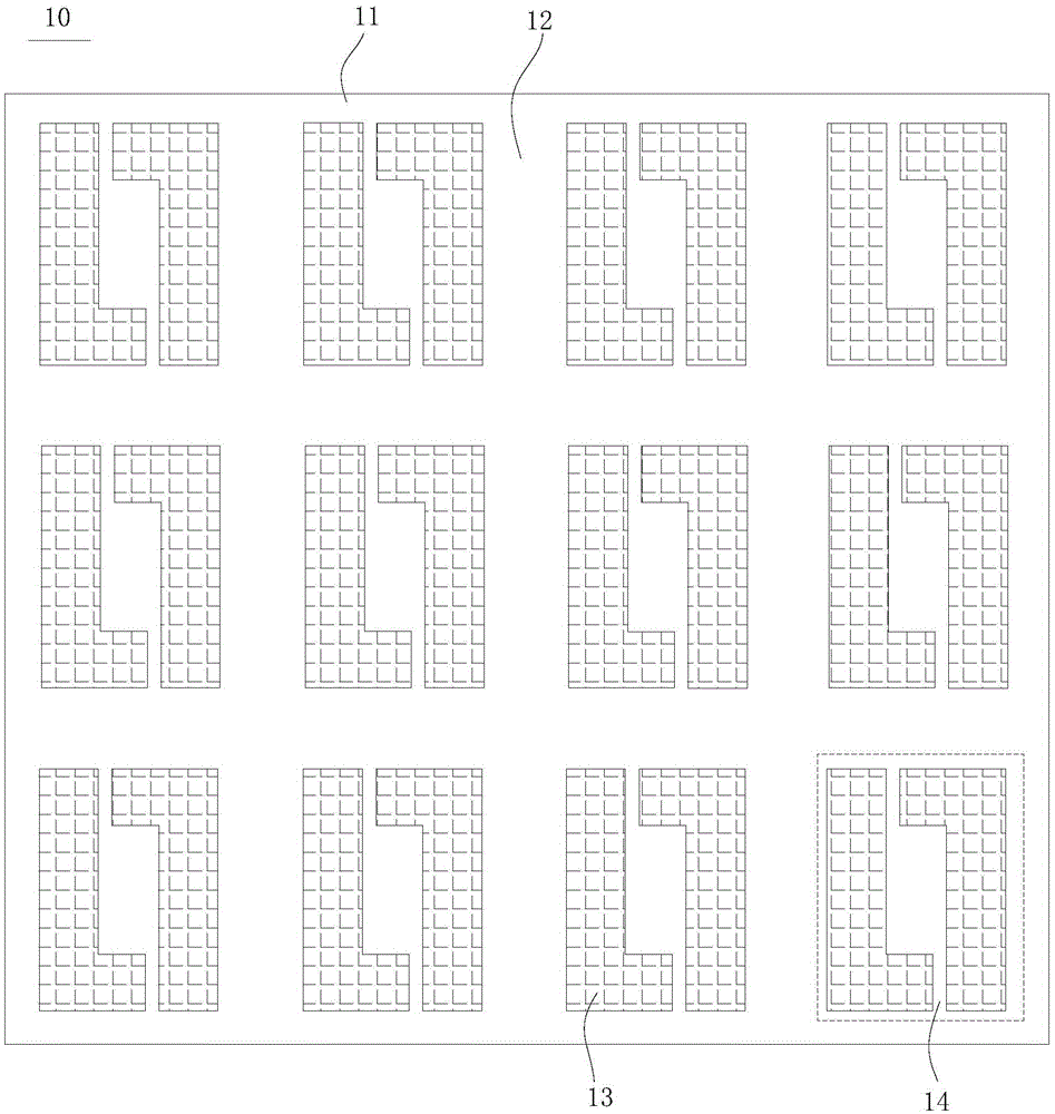
[0023] According to the existing technology, the inner layer circuit (forming the core board) is sequentially processed through cutting → negative film process → pressing, and the base material is made into an undrilled multi-layer board, that is, the inner layer core board, the prepreg and the outer layer of copper Foils are pressed together to form a board; the prepared multi-layer board includes a plurality of module areas, and the module area includes a plurality of areas for forming unit boards, which are called unit board areas. A molding edge with a width of 3.0mm for post-molding is left between each module area (in other embodiments, the width of the molding edge can be determined according to the layout de...


PUM


Abstract

The invention relates to the technical field of circuit board production, and specifically to a manufacturing method for a fine circuit. An overflow hole is drilled in a molding edge of a multi-layered board; residual etching liquid medicine in the middle of the board can flow out of the overflow hole in an etching process so as to accelerate etching liquid medicine exchange, weaken a pool effect and improve the etching capability in order to reduce the lateral-etching quantity and deckle edges, improve the etching uniformity and improve the manufacturing precision of the circuit. By controlling the size and the hole edge distance of the overflow hole, the etching liquid medicine exchanging speed is improved while the increasing risk of board-breaking in the machining process of the multi-layered board due to the existence of the overflow hole is avoided as well; and by controlling alkali etching parameters, the etching effect can be further improved, and the precision of the circuit can be further improved as well.

Description

technical field [0001] The invention relates to the technical field of circuit board production, in particular to a method for manufacturing fine circuits. Background technique [0002] PCB (Printed Circuit Board), the Chinese name is printed circuit board, also known as printed circuit board. The production process of PCB is generally as follows: material cutting→inner layer graphics→inner layer etching→inner layer AOI→browning→pressing→drilling→immersion copper→full board plating→outer layer graphics→graphic plating→outer layer etching→ Outer layer AOI→silk printing solder mask, characters→surface treatment→forming→electrical testing→FQC→packaging. Among them, in order to improve efficiency and facilitate production, multiple unit graphics (unit) will be put together to form a set of module graphics (set); The forming edge formed in the later stage, together with the peripheral process edge, forms a manufacturing unit (panel), the base material is cut according to the si...

Claims


Application Information

Patent Timeline
Patent Type & Authority Applications(China)
IPC IPC(8): H05K3/18
CPCH05K3/188H05K2203/0221H05K2203/0793
Inventor 敖四超白会斌钟宇玲寻瑞平
Owner JIANGMEN SUNTAK CIRCUIT TECH
Why Eureka
Try Eureka