Thyristor chip with seven-layer p-n junction isolation structure and preparation method of thyristor chip

A through isolation, silicon chip technology, applied in the field of thyristor chips, can solve the problems of large isolation area width, increased process difficulty, short diffusion time, etc., and achieves small isolation area width, saving silicon wafer area, and short diffusion time. Effect

Active Publication Date: 2016-06-01
JIANGSU JIEJIE MICROELECTRONICS
View PDF6 Cites 5 Cited by
  • Summary
  • Abstract
  • Description
  • Claims
  • Application Information

AI Technical Summary

Problems solved by technology

[0002] The through isolation structure is widely used in thyristor chips. At present, the existing through isolation structures mainly include boron diffusion through isolation structure and laser perforation vacuum aluminum expansion structure. For example: background technology 1: boron diffusion through isolation technology, the isolation area realize Method: double-sided photolithography isolation window - double-sided boron pre-deposition - high temperature push junction, advantages: fewer production steps, disadvantages: long diffusion time, high production energy consumption, low efficiency, large lateral diffusion on the surface of the isolation area, resulting in Large width, waste of silicon wafer area; background technology 2: laser perforation and then vacuum aluminum expansion technology, isolation area realization method: laser drilling - vacuum closed tube expansion - high temperature push junction, advantages: short diffusion time, simultaneous formation of isolation area, P1 and P2 areas, disadvantages: low efficiency of laser perforation, because the silicon wafer is covered with dense through-holes, which increases the difficulty of the subsequent process, and the silicon wafer has a high breakage rate in the subsequent process

Method used


Image

  • Thyristor chip with seven-layer p-n junction isolation structure and preparation method of thyristor chip
  • Thyristor chip with seven-layer p-n junction isolation structure and preparation method of thyristor chip
  • Thyristor chip with seven-layer p-n junction isolation structure and preparation method of thyristor chip

Examples


Embodiment Construction

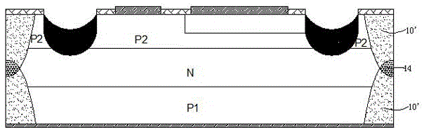
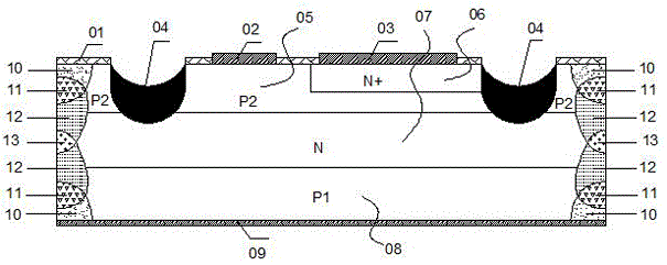
[0016] Such as Figure 4 , 5 A thyristor chip with a seven-layer on-through isolation structure and its preparation method are shown, including an anode region P18, an N-type long base region 7, a short base region P25, an N- + Type cathode region 6 and front oxide film 1, front gate metal electrode 2, front cathode metal electrode 3, back anode metal electrode 9, annular passivation trench 4 and glass passivation filled in the passivation trench chemical film and the isolation ring of the seven-layer isolation structure, the isolation ring of the seven-layer isolation structure is composed of boron impurity region 10, boron, aluminum mixed impurity region 11, aluminum impurity region 12, aluminum-aluminum The overlapping impurity region 13, the aluminum impurity region 12, the boron and aluminum mixed impurity region 11, and the boron impurity region constitute 10, and the isolation ring of the seven-layer through-isolation structure is arranged vertically on the oxide film ...


PUM


Abstract

The invention discloses a thyristor chip with a seven-layer p-n junction isolation structure and a preparation method of the thyristor chip. The thyristor chip comprises an anode region P1, an N-type long base region, a short base region P2, an N<+>-type cathode region, a front oxidation film, a front gate metal electrode, a front cathode metal electrode, a back anode metal electrode, an annular passivation groove and an isolation ring of the seven-layer p-n junction isolation structure, wherein the isolation ring of the seven-layer p-n junction isolation structure comprises a boron impurity region, a boron-aluminum mixed impurity region, an aluminum impurity region, an aluminum-aluminum overlapping impurity region, an aluminum impurity region, the boron-aluminum mixed impurity region and the boron impurity region from top to bottom; and the isolation ring of the seven-layer p-n junction isolation structure is arranged between the front oxidation film and the back anode metal electrode along the vertical direction and surrounds the peripheries of the anode region P1, the N-type long base region and the short base region P2. The thyristor chip is short in diffusion time, low in production energy consumption, high in efficiency, high in silicon wafer integrity rate, little in transverse diffusion of the isolation region surface and small in isolation region width, and saves the area of the silicon wafer.

Description

technical field [0001] The invention relates to a thyristor chip with a seven-layer through isolation structure, in particular to a seven-layer through isolation structure used in the manufacture of a thyristor chip, and provides a preparation method for realizing the thyristor device chip . Background technique [0002] The through isolation structure is widely used in thyristor chips. At present, the existing through isolation structures mainly include boron diffusion through isolation structure and laser perforation vacuum aluminum expansion structure. For example: background technology 1: boron diffusion through isolation technology, the isolation area realize Method: double-sided photolithography isolation window - double-sided boron pre-deposition - high temperature push junction, advantages: fewer production steps, disadvantages: long diffusion time, high production energy consumption, low efficiency, large lateral diffusion on the surface of the isolation area, resul...

Claims


Application Information

Patent Timeline
Patent Type & Authority Applications(China)
IPC IPC(8): H01L29/06H01L29/747H01L21/328
CPCH01L29/0603H01L29/0684H01L29/66363H01L29/747
Inventor 沈怡东王成森周榕榕
Owner JIANGSU JIEJIE MICROELECTRONICS
Why Eureka
Try Eureka