RFLDMOS device and manufacturing method thereof

A manufacturing method and device technology, applied in semiconductor/solid-state device manufacturing, semiconductor devices, electrical components, etc., can solve the problems of snapback effect, device voltage failure, poor robustness, etc., achieve large breakdown voltage, avoid The effect of failure of pressure resistance and improvement of robustness

Active Publication Date: 2016-06-01
SHANGHAI HUAHONG GRACE SEMICON MFG CORP
View PDF5 Cites 0 Cited by
  • Summary
  • Abstract
  • Description
  • Claims
  • Application Information

AI Technical Summary

Problems solved by technology

The structure of this RFLDMOS device has only one layer of P epitaxy 2. In order to ensure that the device has a large breakdown voltage BV, the doping concentration of P epitaxy 2 is generally low, which makes the base resistance R B Difficult to reduce, snapback effect may occur, causing tube burnout and other device voltage resistance failures, poor robustness

Method used


Image

  • RFLDMOS device and manufacturing method thereof
  • RFLDMOS device and manufacturing method thereof
  • RFLDMOS device and manufacturing method thereof

Examples


Embodiment 1

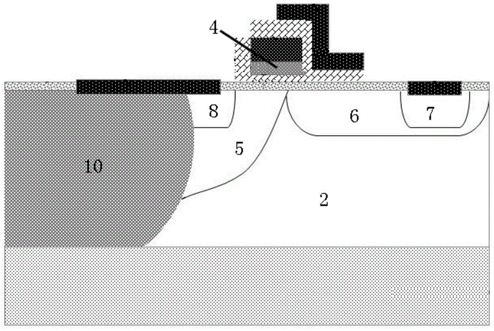
[0064] RFLDMOS (Radio Frequency Laterally Diffused Metal Oxide Semiconductor) devices such as image 3 as shown,

[0065] A first layer of P epitaxy 21 is formed on the P substrate 1;

[0066] A second layer P epitaxy 22 is formed on the first layer P epitaxy 21;

[0067] In the second layer P epitaxy 22, a P well 3 is formed in the left part, and a drain N-type lightly doped region 4 is formed in the right part;

[0068] The drain N-type lightly doped region 4 has a drain N-type heavily doped region 5 formed on the right;

[0069] The P well 3 is connected to a contact column 7 on the left side, and a source terminal N-type heavily doped region 6 is formed in the middle;

[0070] The contact column 7 is connected to the second layer P epitaxy 22, the first layer P epitaxy 21 and the P substrate 1;

[0071] A bulk P-type heavily doped region 8 communicating with the contact pillar 7 is formed on the upper part of the P well 3 on the left side of the N-type heavily doped re...

Embodiment 2

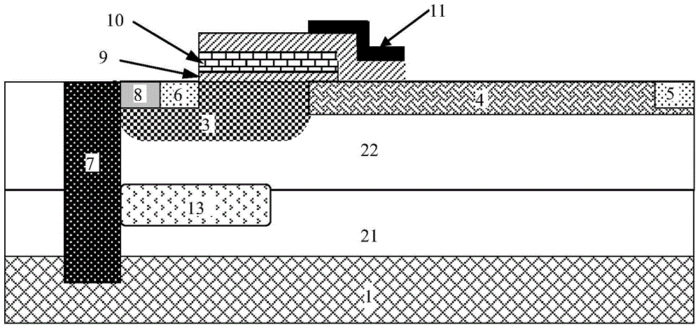
[0090] A method for manufacturing an RFLDMOS (radio frequency laterally diffused metal oxide semiconductor) device, comprising the following steps:

[0091] One. grow the first layer of P epitaxy 21 on the P substrate 1, as Figure 4 shown;

[0092] 2. Photolithography, carry out P-type ion implantation in the first layer P epitaxy 21, form P buried layer (PBuriedLayer), as Figure 5 shown;

[0093] 3. Remove photoresist 15, form second layer P epitaxy 22 on first layer P epitaxy 21, as Figure 6 shown;

[0094] The P-type doping concentration of the first layer P epitaxy 21 is greater than the P-type doping concentration of the second layer P epitaxy 22;

[0095] 4. Forming P well 3, drain N-type lightly doped region 4, source N-type heavily doped region 6, bulk P-type heavily doped region 8, drain N-type heavily doped region 5, gate oxide 9, Polysilicon gate 10, Faraday shield (Faradayshield) 11, metal contact post 7, such as image 3 shown;

[0096] P well 3 is forme...


PUM


Abstract

The invention discloses an RFLDMOS device. Two P epitaxial layers of different P doping concentrations are formed on a P substrate, wherein the P doping concentration of a first P epitaxial layer at the bottom thereof is relatively large and the P doping concentration of a second P epitaxial layer at the top thereof is relatively small. Meanwhile, a P buried layer is formed in the P epitaxial layers from a contact column to be below a polysilicon gate. The P doping concentration of the second P epitaxial layer in a P type channel region is relatively small, so that the large breakdown voltage of the RFLDMOS device is ensured. At the same time, since the P doping concentration of the first P epitaxial layer at the bottom thereof is relatively large, the base resistance of a parasitic NPN tube formed by a drain drift region, the P type channel region and a source region is greatly reduced due to the existence of the P buried layer larger than the P doping concentration of the above P epitaxial layer. Therefore, the snapback effect is avoided, and the robustness of the RFLDMOS device is improved. The invention also discloses a manufacturing method of the RFLDMOS device.

Description

technical field [0001] The invention relates to semiconductor technology, in particular to an RFLDMOS device and a manufacturing method thereof. Background technique [0002] More than 10 years ago, LDMOS (Laterally Diffused Metal Oxide Semiconductor) products began to gradually advance in the radio frequency field as a substitute for bipolar transistors. [0003] RFLDMOS (Radio Frequency Laterally Diffused Metal Oxide Semiconductor) device is a new generation of integrated solid-state microwave power semiconductor product formed by the integration of semiconductor integrated circuit technology and microwave electronic technology. It has good linearity, high gain, high withstand voltage and high output power. , good thermal stability, high efficiency, good broadband matching performance, easy to integrate with MOS process, etc., and its price is much lower than that of gallium arsenide devices. It is a very competitive power device and is widely used in GSM, PCS, power ampl...

Claims


Application Information

Patent Timeline
Patent Type & Authority Applications(China)
IPC IPC(8): H01L29/78H01L29/06H01L21/336
Inventor 徐向明黄景丰
Owner SHANGHAI HUAHONG GRACE SEMICON MFG CORP
Why Eureka
Try Eureka