Automatic alignment method based on Cadence Via

An automatic alignment and PCB board technology, applied in special data processing applications, instruments, electrical digital data processing, etc., can solve the problems of occupying PCB board space, destroying the appearance of the board, affecting the PCB board, etc., to achieve a beautiful layout , Improve the utilization rate of boards and cards, and facilitate the operation

Inactive Publication Date: 2016-06-08
INSPUR GROUP CO LTD
View PDF2 Cites 3 Cited by
  • Summary
  • Abstract
  • Description
  • Claims
  • Application Information

AI Technical Summary

Problems solved by technology

There are many vias on the PCB board, usually there are scattered vias, scattered layout, etc., occupying a lot of space on the PCB board, which seriously affects the design of the net on the PCB board, and also destroys the appearance of the board.

Method used


Image

  • Automatic alignment method based on Cadence Via
  • Automatic alignment method based on Cadence Via

Examples


Embodiment 1

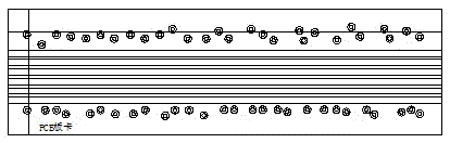
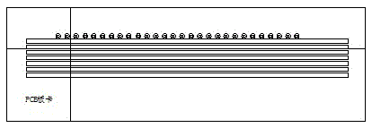
[0019] A kind of method based on CadenceVia automatic alignment described in this embodiment, in CadenceLayout design, by revising the partial configuration file of the SKILL program of automatic alignment Via in the PCB board, put this SKILL program into Skill menu then, and execute this The SKILL program directly modifies the background database designed by Layout, and can change the position of the original Via with one key, so that the Via can be automatically aligned with one key.

[0020] Using the method for automatic alignment based on CadenceVia described in this embodiment, its specific implementation steps include:

[0021] 2) Select the Via that needs to be changed currently;

[0022] 2) Choose a Via as a basic point;

[0023] 3) Select the spacing and position of the required Via according to the design requirements;

[0024] 4) Run SKILL, Via will automatically change to the desired position;

[0025] 5) Run the SKILL operation and output the Done command.

...


PUM


Abstract

The invention discloses an automatic alignment method based on Cadence Via, and relates to the technical field of EDA. A SKILL set program for automatic alignment of Via in a PCB is written and set, then, the SKILL program is put into a SKILL menu, the original position of Via can be changed in a one-key mode by executing the SKILL program, and one-key automatic alignment is achieved. By adopting the automatic alignment method, the Via interval in the PCB is uniform, the layout is more attractive compared with the prior art, the net setting space is enlarged, and the board card utilization rate is increased.

Description

technical field [0001] The invention relates to the technical field of EDA, specifically a method for automatic alignment based on CadenceVia. Background technique [0002] With the development of society, people's requirements for electronic products are getting higher and higher. In order to cater to and satisfy the public's psychology, the electronic information industry is also conducting continuous research and practice, developing new electronic products, and promoting the development of the information age. . As the cornerstone of development, PCB board design requires continuous improvement and innovation. [0003] At present, in the design of PCB boards, in double-sided and multi-layer boards, in order to connect the printed wires between the layers, a common hole, that is, a via hole, is drilled at the intersection of the wires that need to be connected in each layer. The hole itself has a parasitic capacitance to the ground, as well as a parasitic inductance, wh...

Claims


Application Information

Patent Timeline
Patent Type & Authority Applications(China)
IPC IPC(8): G06F17/50
CPCG06F30/392
Inventor 刘金凤张得文李晓
Owner INSPUR GROUP CO LTD
Why Eureka
Try Eureka