Device for detecting two-dimensional morphology of wafer substrate

A wafer and substrate technology, which is applied in the field of devices for detecting the two-dimensional topography of wafer substrates, can solve the problems of system error, influence consistency, complex structure of the light-transmitting device, etc., and achieve high coating precision, ensure consistency and simple structure Effect

Active Publication Date: 2016-06-22
NANCHANG ANGKUN CO LTD
View PDF7 Cites 2 Cited by
  • Summary
  • Abstract
  • Description
  • Claims
  • Application Information

AI Technical Summary

Problems solved by technology

Due to the relatively complex structure of the light-passing device and its own system error, it is difficult to ensure the consistency of the light received by each PSD
In addition, in thi

Method used


Image

  • Device for detecting two-dimensional morphology of wafer substrate
  • Device for detecting two-dimensional morphology of wafer substrate
  • Device for detecting two-dimensional morphology of wafer substrate

Examples


Example Embodiment

[0015] Example 1

[0016] For ease of understanding, Embodiment 1 of the present invention only provides one of the light beams in the first direction and the light beam in the second direction.

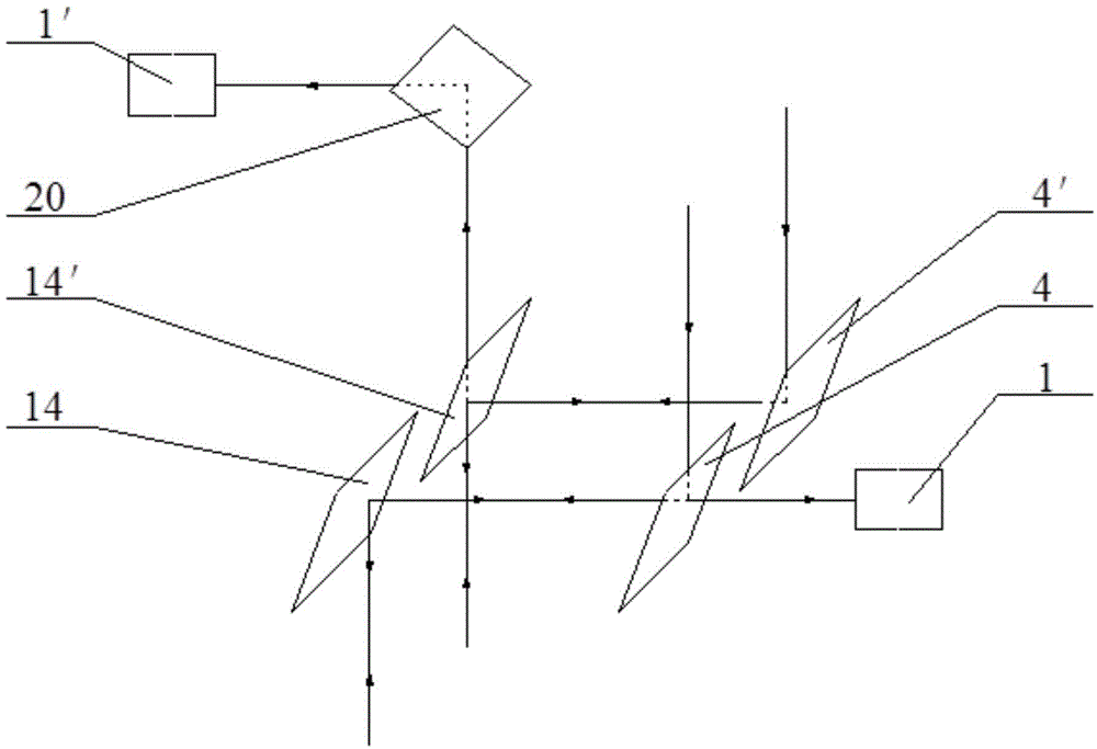
[0017] see attached figure 1 , the device for detecting the two-dimensional topography of the wafer substrate provided by the first embodiment of the present invention includes N PSD1 or 1', N laser beams, N first beam splitters 4 or 4' corresponding to the N laser beams one-to-one, and N beams of laser light. There are N second beam splitters 14 or 14' corresponding to the laser beams one-to-one, and the N beams of lasers are arranged in a straight line, wherein N is a natural number above 3, and the N PSD1 or 1' correspond to the N beams of lasers one-to-one, and N PSD1 or 1' are arranged on the left and right sides of the N-beam laser respectively, including the left PSD1' and the right PSD1,

[0018] Each laser beam is incident on the second beam splitter 14 or 14' after passin...

Example Embodiment

[0035] Embodiment 2

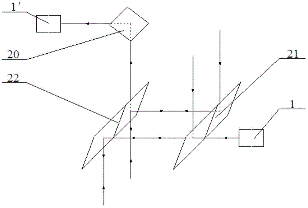
[0036] see attached figure 2 , which is different from the device for detecting the two-dimensional topography of the wafer substrate provided by the first embodiment of the present invention is that in the device for detecting the two-dimensional topography of the wafer substrate provided by the second embodiment of the present invention, there are one-to-one correspondence with the N laser beams. The N first beam splitters 4 or 4' and / or the N second beam splitters 14 or 14' corresponding to the N laser beams are integrated into one piece, respectively. figure 2 Among them, the N first beam splitters are integrated into one piece, and the number is 21, and the N second beam splitters are integrated into one piece, and the number is 22; corresponding to the area of ​​the light beam in the first direction, the coating of the first beam splitter 21 makes it in ( The reflectivity in the wavelength range of λ-10nm, λ+10nm) is 50%, which corresponds to the...

Example Embodiment

[0042] Embodiment 3

[0043] see attached Figure 4 and attached Figure 5 , the difference from the device for detecting the two-dimensional topography of a wafer substrate provided by the third embodiment of the present invention is that in the device for detecting the two-dimensional topography of a wafer substrate provided by the third embodiment of the present invention, the N beams of laser light are composed of a multi-channel laser. The transmitter emits.

[0044] The multiplex laser emitting device includes a multiplex beam splitter prism 37 and a laser 36, the multiplex beam splitter prism 37 includes a plurality of beam splitting surfaces, the multiple beam splitting surfaces are parallel, and the included angles α between the multiple beam splitting surfaces and the horizontal direction are respectively 45°, The centers of the multiple beam splitting surfaces are on the same straight line, and the laser light emitted by the laser 36 is directed to one of the oute...


PUM


Abstract

The invention provides a device for detecting the two-dimensional morphology of a wafer substrate, and belongs to the technical field of semiconductor material nondestructive testing. The device for detecting the two-dimensional morphology of a wafer substrate comprises N first beam splitters in one-to-one correspondence with N laser beams and N second beam splitters in one-to-one correspondence with N laser beams. The N first beam splitters and the N second beam splitters are provided with coating areas, the coating areas make the beam splitters different in reflectance and transmittance, so that N beams of light incident on a sample and then returned can be divided into two directions through the first beam splitters and the second beam splitters and detected separately. The reflectance and transmittance properties of each coating area are determined by the propagation direction of corresponding first-type reflected light beams. By coating different areas of the beam splitters with films of different properties, the requirement of the device for detecting the two-dimensional morphology of a wafer substrate for light path transmission is met. As the coating precision is extremely high, the consistency of light received by PSDs in different propagation directions is ensured.

Description

technical field [0001] The invention relates to the technical field of non-destructive testing of semiconductor materials, in particular to a device for detecting the two-dimensional topography of a wafer substrate. Background technique [0002] The invention patent application with application number 201410189094.1 relates to a device for rapid real-time detection of the two-dimensional topography of a wafer substrate, including N PSDs, N laser beams and a first spectroscopic element, the N laser beams are arranged along a straight line, wherein, all the The N is a natural number greater than or equal to 3, the N PSDs are in one-to-one correspondence with N laser beams, and the N beams of laser light are first emitted to the first beam splitting element, and then the incident light is formed after passing through the first beam splitting element. The incident light is incident on the wafer base, and N incident points are formed on the wafer base along the radial direction. ...

Claims


Application Information

Patent Timeline
IPC IPC(8): G01B11/245
Inventor 刘健鹏黄文勇张瑭张立芳
Owner NANCHANG ANGKUN CO LTD
Why Eureka
Try Eureka