
Eureka
For R&D, Eureka makes reading and utilizing patents & technical documents easy.
Eureka AIR
Designed for self-driven R&D workflows. Generate viable solutions, solve complex R&D challenges, empower your innovation with AI.

Eureka Materials
Designed for material experts only. Revolutionize your material R&D, from search, analyze, to developing new materials.

TechResearch
Generate reliable direction feasibility study reports for your R&D in just a few steps.

TechSeek
Discover and master advanced knowledge NOW. Basics, ideas, possibilities, all at once.

TechMind
As an expert in R&D Theories, TechMind can generates customized viable solutions instantly.

TechRisk
Analyze your overall solution with one click, know your potential R&D risks in advance.

TechMonitor
Get weekly tech updates, stay abreast of the latest tech innovations and key insights.
Chemical field effect transistor gas-sensitive sensor and manufacturing method thereof
A field effect transistor, gas sensor technology, applied in the sensor field, can solve problems such as high manufacturing cost
- Summary
- Abstract
- Description
- Claims
- Application Information
AI Technical Summary
Problems solved by technology
Method used
Image

Examples
Embodiment Construction
[0042] The present invention will be described in detail below with reference to embodiments of the invention shown in the accompanying drawings. However, the idea of the invention should not be limited to these examples, nor are these the only possible forms in which the invention can be implemented. It should be considered that different implementations that can achieve the same or equivalent functions are also included within the spirit and scope of the present invention. Further, these embodiments will disclose the present invention in detail and comprehensively, and fully convey the protection scope of the present invention to those skilled in the art.
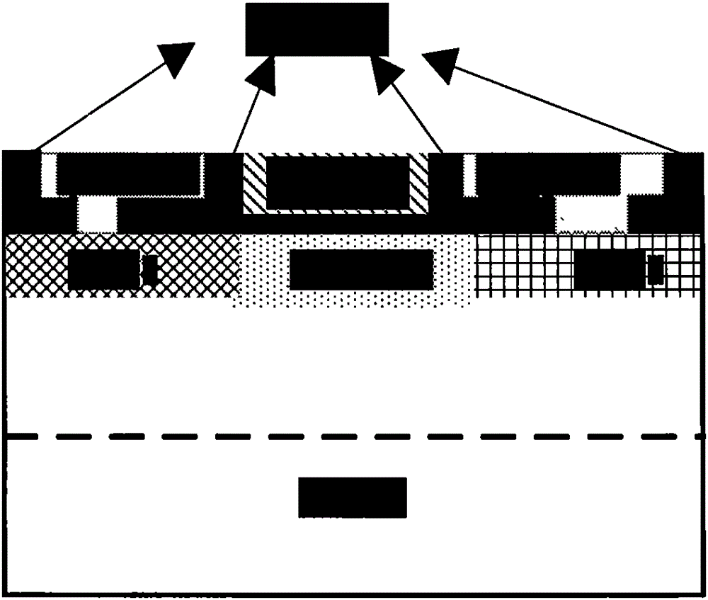
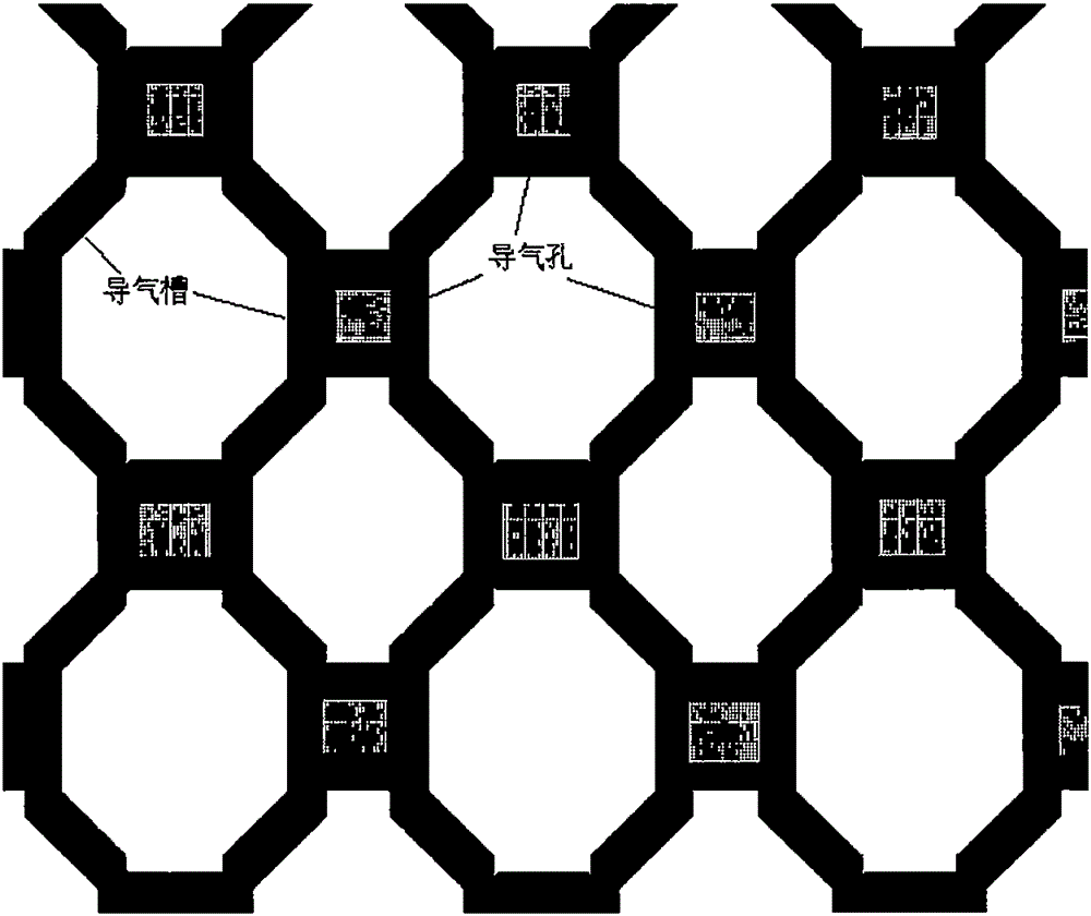
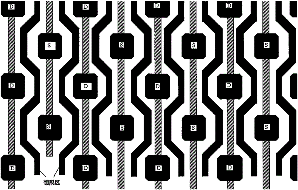
[0043] figure 1 It is a structural schematic diagram of the MOSFET chemical sensor of the present invention. The source and drain regions of the device are made on the semiconductor substrate, and then the sensitive layer is made on the gate insulating layer by sputtering, deposition, self-assembly and other physical ...
PUM
| Property | Measurement | Unit |
|---|---|---|
| thickness | aaaaa | aaaaa |
Abstract
Description
Claims
Application Information
 - R&D Engineer
- R&D Manager
- IP Professional
- Industry Leading Data Capabilities
- Powerful AI technology
- Patent DNA Extraction
Browse by: Latest US Patents, China's latest patents, Technical Efficacy Thesaurus, Application Domain, Technology Topic, Popular Technical Reports.
© 2024 PatSnap. All rights reserved.Legal|Privacy policy|Modern Slavery Act Transparency Statement|Sitemap|About US| Contact US: help@patsnap.com