

Preparation method for TEM sample
A sample and equipment technology, applied in the field of TEM sample preparation, can solve problems such as difficult to control the processing process accurately, sample damage, rough surface, etc., and achieve the effect of shortening the sample preparation time and improving the success rate
- Summary
- Abstract
- Description
- Claims
- Application Information
AI Technical Summary
Problems solved by technology
Method used
Image

Examples
Embodiment Construction
[0035] The specific embodiment of the present invention will be further described in detail below in conjunction with the accompanying drawings.
[0036] It should be noted that, in the following specific embodiments, when describing the embodiments of the present invention in detail, in order to clearly show the structure of the present invention for the convenience of description, the structures in the drawings are not drawn according to the general scale, and are drawn Partial magnification, deformation and simplification are included, therefore, it should be avoided to be interpreted as a limitation of the present invention.
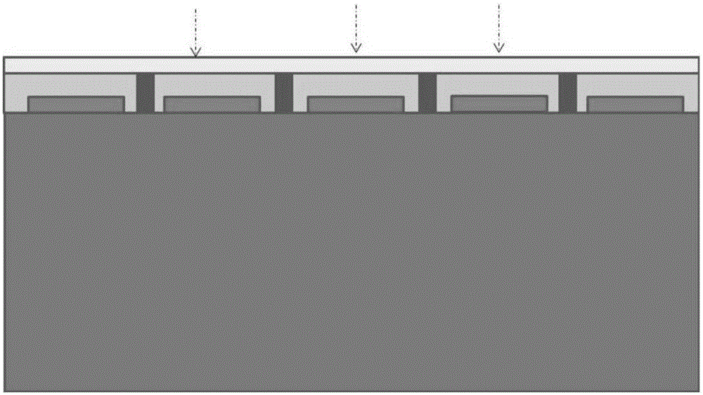
[0037] In the following specific embodiments of the present invention, please refer to image 3 , image 3 It is a flow chart of the preparation method of a TEM sample of the present invention; meanwhile, please refer to Figure 4-Figure 7 , Figure 4-Figure 7 is a preferred embodiment of the present invention according to image 3 Schematic diag...
PUM
 Abstract
Description
Claims
Application Information