SIP chip and laser device coupling method and optical transceiver module manufactured with same

An optical transceiver module and laser technology, applied in the field of communications, can solve the problems of SIP chips and lasers, unfavorable mass production operations, low production efficiency, etc., and achieve the effects of easy mass production operations, simple structure, and high production efficiency.

Active Publication Date: 2016-06-29
GUANGXUN SCI & TECH WUHAN
View PDF3 Cites 5 Cited by
  • Summary
  • Abstract
  • Description
  • Claims
  • Application Information

AI Technical Summary

Problems solved by technology

[0007] The optical fiber connection on the SIP chip, especially in the coupling range and at the joint of the transceiver module port, the optical fiber is a bare fiber with the coating removed. During the coupling and packaging process, the optical fiber is prone to breakage and damage
[0008] When the SIP chip integrated with the Mach-Zander (MZ) modulator is coupled with the output fiber of the laser, there is a requirement for the polarization state, that is, only linearly polarized light in a specific direction can be transmitted in the SIP chip with the minimum loss. Usually, the The method is active coupling, that is, powering the laser and the SIP chip during the coupling process, and judging whether the polarization state of the incident light is optimal for coupling by monitoring the output optical power. This method is cumbersome and has low production efficiency. Facilitate large-scale production operations
[0009] When the SIP chip and laser are working, they will inevitably generate heat. If the generated heat is not conducted away in time, the heat will accumulate, which will increase the temperature of the SIP chip and laser when they are working, causing the SIP chip and laser to interact with each other. Performance worsening and shortened lifespan

Method used


Image

  • SIP chip and laser device coupling method and optical transceiver module manufactured with same
  • SIP chip and laser device coupling method and optical transceiver module manufactured with same
  • SIP chip and laser device coupling method and optical transceiver module manufactured with same

Examples


Embodiment Construction

[0046] The present invention will be described in detail below in conjunction with the drawings and embodiments.

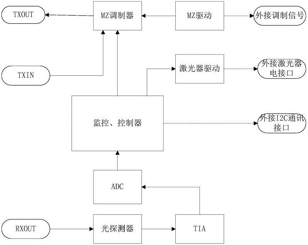
[0047] SIP chip 3 is a silicon-based optoelectronic chip that integrates Mach-Zander (MZ) modulators, photodetectors, and internal diagnostic and control processors in integrated circuits. The internal functional structure of the SIP chip is as follows: figure 1 As shown, it can control the laser to work, and accept external information to modulate the optical signal at 2.5Gpbs-25Gpbs, and can also accept the external 2.5Gpbs-25Gpbs modulated optical information to convert it into an electrical signal.

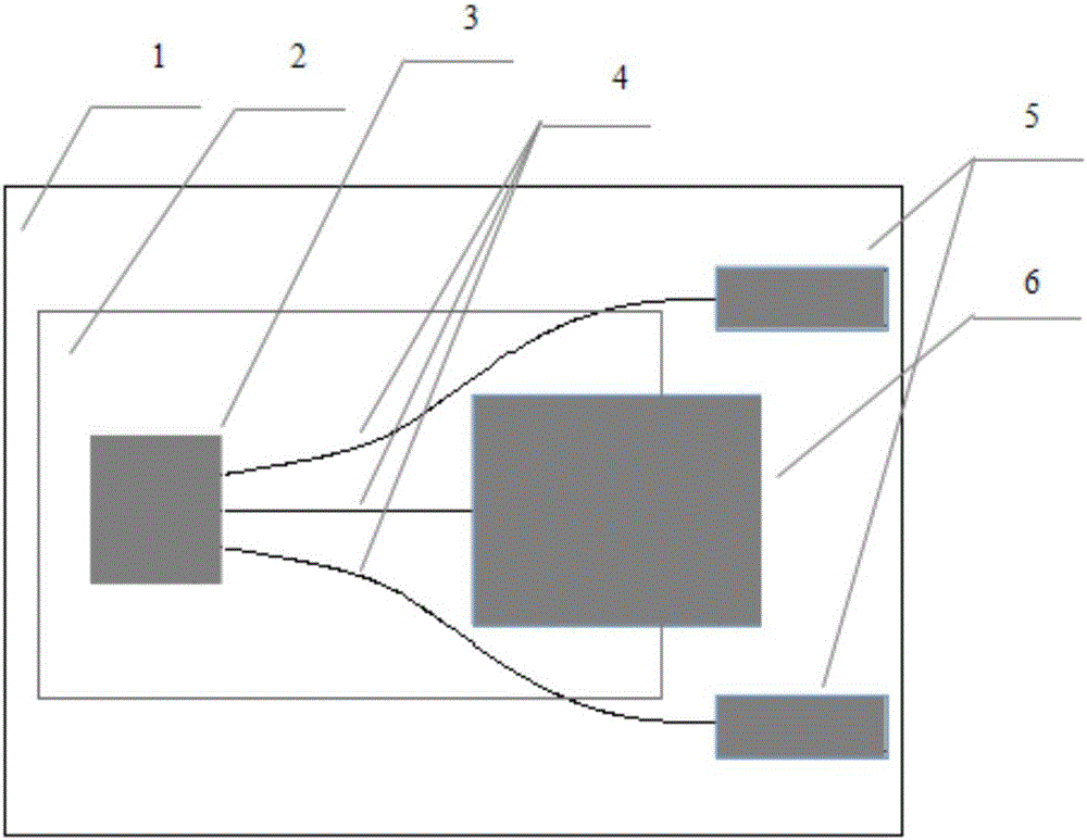
[0048] Embodiments of the present invention provide a structure of an optical transceiver module with a built-in silicon-based optoelectronic chip (SIP), which is a small pluggable structure (SFP), such as figure 2 As shown, it includes substrate 1, circuit board 2, SIP chip 3, optical fiber 4, LC optical interface 5, laser 6, spacer 8,

[0049] Substrate 1 carr...


PUM


Abstract

The invention provides a SIP chip and laser device coupling method and an optical transceiver module manufactured with the same.The coupling method comprises the step of making a laser device (6) aligned with the polarization direction required by a SIP chip (3), wherein a cross curve of the X axis and Y axis of a SIP chip coupling port is found by means of an image visual system, a cross curve formed by the X axis and Y axis of the light emitting end face (6-2-1) of a laser device chip (6-2) is marked on the bottom surface of a TO tube socket for encapsulating the laser device chip in an equivalent mode, then the image visual system is made to face the bottom surface of the TO tube socket of the laser device, and the position of the laser device is adjusted to enable the cross curve on the bottom surface of the TO tube socket to be aligned with the cross curve on the image visual system.Passive coupling is conducted by means of the image visual system during optical module coupling, production efficiency is high, and large-scale production can be achieved easily; the optical module is simple in structure and small in size and can be encapsulated in a small form-factor pluggable (SFP) structure; structural integration is realized, and fiber breaking does not occur easily; heat dissipation property is high, and reliability is high.

Description

technical field [0001] The invention relates to an optical communication device, in particular to a method for coupling a SIP chip and a laser and an optical transceiver module composed thereof, and the invention belongs to the field of communication. Background technique [0002] In the optical transceiver module, according to the relationship between the modulation mode and the light source, the laser light source is divided into two types: direct modulation and external modulation. Because external modulation is to change the parameters of the output laser, the requirements for laser characteristics are not high, and it is suitable for high-speed (2.5Gbps-40Gbps), long-distance optical communication, people pay more attention and attention to the development of external modulation optical transceiver modules . Currently, electro-absorption externally modulated lasers (EML) are mostly used in long-distance and high-speed optical transceiver modules (such as SFP+ modules)....

Claims


Application Information

Patent Timeline
Patent Type & Authority Applications(China)
IPC IPC(8): G02B6/42G02B6/36
CPCG02B6/3636G02B6/4224G02B6/4243
Inventor 马洪勇宋琼辉杜巍陈强穆磊宋蓓莉马卫东
Owner GUANGXUN SCI & TECH WUHAN
Why Eureka
Try Eureka