Silicon-based gallium nitride epitaxial structure and manufacturing method thereof

A technology of epitaxial structure and manufacturing method, which is applied in semiconductor/solid-state device manufacturing, electrical components, circuits, etc., can solve the problems of silicon-based gallium nitride epitaxial cracks and insignificant effects of bending, so as to reduce stress and reduce position The effect of error density and performance improvement

Inactive Publication Date: 2016-06-29
梁辉南 +2
View PDF7 Cites 11 Cited by
  • Summary
  • Abstract
  • Description
  • Claims
  • Application Information

AI Technical Summary

Problems solved by technology

Therefore, the effect of eliminating epitaxial cracks and

Method used


Image

  • Silicon-based gallium nitride epitaxial structure and manufacturing method thereof
  • Silicon-based gallium nitride epitaxial structure and manufacturing method thereof

Examples


Example Embodiment

[0033] Embodiment one

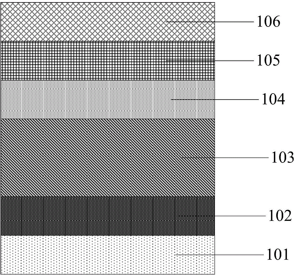
[0034] This embodiment describes a GaN-on-Si epitaxial structure. The silicon-based GaN epitaxial structure described in this embodiment is subsequently applied to GaN power devices.

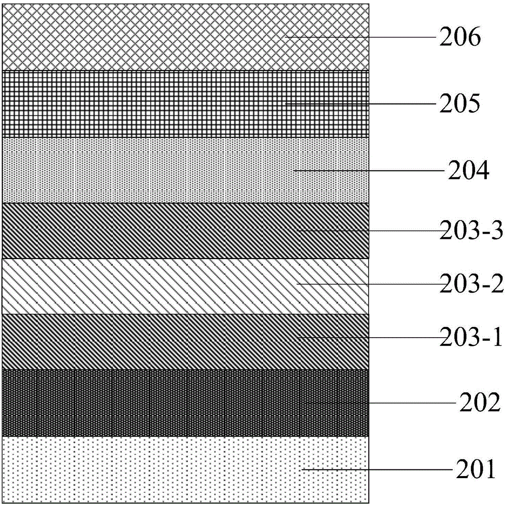
[0035] figure 2 A schematic structural diagram of the GaN-on-Si epitaxial structure of this embodiment is shown. like figure 2 As shown, the GaN-on-Si epitaxial structure includes a silicon substrate 201, the (111) crystal plane of the silicon substrate is used as the growth surface of the subsequent structure, and the (111) crystal plane of the silicon substrate 201 has been nitrided Processing: an aluminum nitride buffer layer 202 is grown on the (111) crystal plane of the silicon substrate, and the aluminum nitride buffer layer 202 and the layers grown as described below are prepared by metal-organic chemical vapor deposition.

[0036] The GaN-on-Si epitaxial structure further includes a first graded buffer layer 203-1 on the aluminum nitride buffer layer 202, th...

Example Embodiment

[0046] Embodiment two

[0047] This embodiment describes a method for manufacturing a GaN-on-Si epitaxial structure.

[0048] The manufacturing method of the GaN-on-Si epitaxial structure provided in this embodiment includes the following steps: first, a silicon substrate is provided, and the (111) crystal plane of the silicon substrate 201 is subjected to nitriding treatment, and the nitriding treatment is carried out at Metal-organic chemical vapor deposition is carried out at a temperature of 900-1100° C. and a pressure of 30-60 Torr in a reaction furnace.

[0049]Then, an aluminum nitride buffer layer 202 is grown on the (111) crystal plane of the silicon substrate by metal-organic chemical vapor deposition at a temperature of 1000-1200° C. and a pressure of 30-60 Torr.

[0050] Next, the first buffer layer 203-1 is grown on the aluminum nitride buffer layer by metal-organic chemical vapor deposition at a temperature of 900-1100° C. and a pressure of 30-60 Torr. The first...


PUM

PropertyMeasurementUnit
Thicknessaaaaaaaaaa
Growth thicknessaaaaaaaaaa

Abstract

The invention provides a silicon-based gallium nitride epitaxial structure and a manufacturing method thereof. The silicon-based gallium nitride epitaxial structure comprises a silicon substrate, including a nitrided surface; an aluminum nitride buffer layer grown on the silicon substrate; a first gradient buffer layer on the aluminum nitride buffer layer and of a multi-layer AlxGal-xN (0.1</=X</=0.9) structure, wherein the X value of each layer AlxGal-xN structure gradually decreases in a direction from adjacent to the aluminum nitride buffer layer to far from the aluminum nitride buffer layer in the multi-layer; a second gradient buffer layer of a multi-layer AlxGal-xN structure, wherein the X value of each layer AlxGal-xN structure gradually increases in a direction from adjacent to the first gradient buffer layer to far from the first gradient buffer layer in the second gradient buffer layer; and a third gradient buffer layer of a multi-layer AlxGal-xN structure, wherein the X value of each layer AlxGal-xN structure has the same change trend as that of the first gradient buffer layer. The silicon-based gallium nitride epitaxial structure provided by the invention can effectively reduce the stress in the epitaxial process, and reduce the generation of cracks.

Description

technical field [0001] The invention relates to the field of semiconductor materials, in particular to a silicon-based gallium nitride epitaxial structure applied to power devices and a manufacturing method thereof. Background technique [0002] Due to the advanced characteristics of GaN material itself, GaN power devices can further reduce the energy conversion process by about 30%- 50% energy loss, while its volume is smaller (1 / 10), its operating voltage is higher (>600V), its conversion power is larger (>kW), and its operating frequency is faster (>50MHz). All these advantages can be transformed into huge economic benefits through commercialization to reduce production costs, making a significant contribution to world energy conservation and consumption reduction. [0003] The core of the entire GaN power device technology is how to produce high-quality GaN materials. Because gallium nitride material itself has a high melting point, it is difficult to use molt...

Claims


Application Information

Patent Timeline
IPC IPC(8): H01L29/06H01L29/205H01L29/207H01L21/02H01L33/12H01L33/32
Inventor 梁辉南
Owner 梁辉南
Why Eureka
Try Eureka