Optical imaging lens group, image capturing device and electronic device

An optical imaging and lens group technology, applied in optics, optical components, instruments, etc., can solve the problems of stray light around the image, reduce the sensitivity of the optical system, and large changes in the refraction of incident light

Active Publication Date: 2016-07-06
LARGAN PRECISION
View PDF7 Cites 12 Cited by
  • Summary
  • Abstract
  • Description
  • Claims
  • Application Information

AI Technical Summary

Problems solved by technology

[0003] Traditional high-resolution miniaturized photographic lenses mounted on electronic devices mostly adopt a four-piece lens structure. The popularity of high-end mobile devices has led to higher requirements for miniaturized camera lenses in terms of pixels and image quality. The existing four-element lens group will not be able to meet higher-level requirements.
[0004] At present, although there is a general traditional five-chip optical system, the uneven distribution of refractive power in the existing optical system is likely to cause excessive changes in the refraction of incident light, which in turn makes it easy to generate stray light around the image, and it is also easy to make the optical system The back focal length is too long, which is not conducive to the miniaturization of the optical system
Further, it may cause the refractive power to be excessively concentrated in a single lens, which hinders the reduction of the sensitivity of the optical system

Method used


Image

  • Optical imaging lens group, image capturing device and electronic device
  • Optical imaging lens group, image capturing device and electronic device
  • Optical imaging lens group, image capturing device and electronic device

Examples


no. 1 example

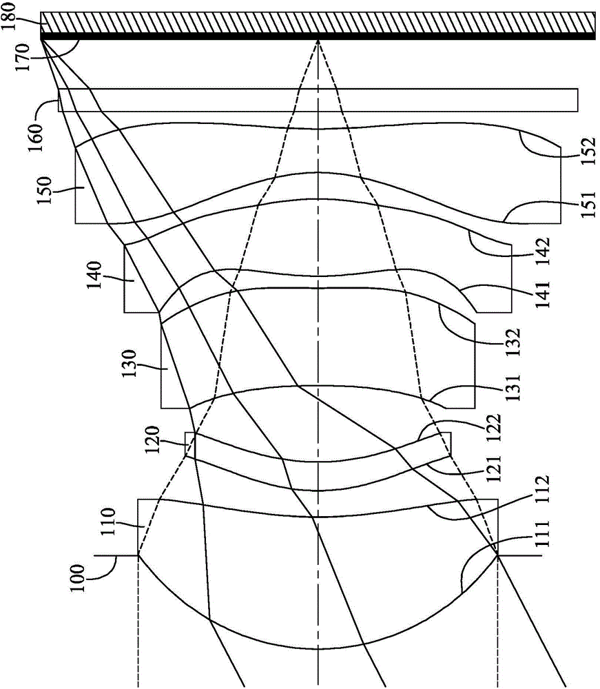
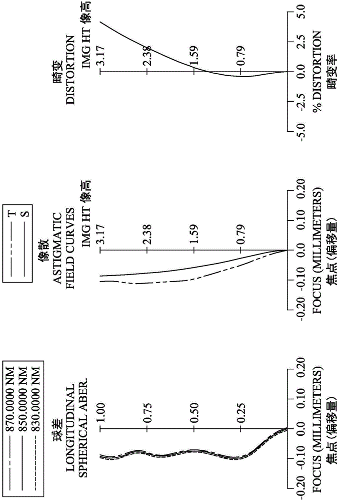
[0114] Please refer to figure 1 and figure 2 ,in figure 1 A schematic diagram of an imaging device according to a first embodiment of the present invention is shown, figure 2 From left to right are the spherical aberration, astigmatism and distortion curves of the first embodiment. Depend on figure 1 It can be seen that the image capturing device includes an optical imaging lens group (not another number) and an electronic photosensitive element 180 . The optical imaging lens group sequentially includes an aperture 100, a first lens 110, a second lens 120, a third lens 130, a fourth lens 140, a fifth lens 150, a filter element (Filter) 160 and an imaging lens from the object side to the image side. Surface 170. Wherein, the electronic photosensitive element 180 is disposed on the imaging surface 170 . There are five single non-bonded lenses with refractive power in the optical imaging lens group (110-150). There is an air space between any two adjacent lenses among th...

no. 2 example

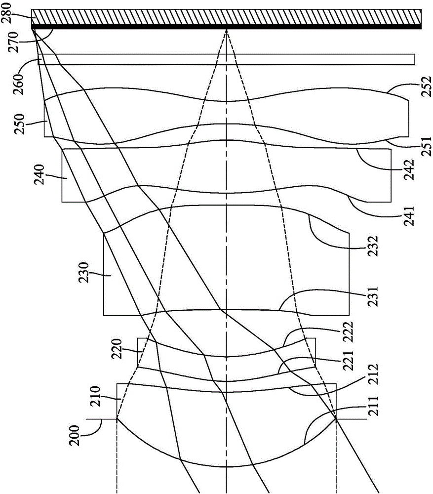
[0146] Please refer to image 3 and Figure 4 ,in image 3 A schematic diagram of an imaging device according to a second embodiment of the present invention is shown, Figure 4 From left to right are the spherical aberration, astigmatism and distortion curves of the second embodiment. Depend on image 3 It can be seen that the image capturing device includes an optical imaging lens group (not another number) and an electronic photosensitive element 280 . The optical imaging lens group sequentially includes an aperture 200 , a first lens 210 , a second lens 220 , a third lens 230 , a fourth lens 240 , a fifth lens 250 , a filter element 260 and an imaging surface 270 from the object side to the image side. Wherein, the electronic photosensitive element 280 is disposed on the imaging surface 270 . There are five single non-bonded lenses with refractive power in the optical imaging lens group (210-250). There is an air space between any two adjacent lenses among the first ...

no. 3 example

[0161] Please refer to Figure 5 and Figure 6 ,in Figure 5 A schematic diagram of an imaging device according to a third embodiment of the present invention is shown, Figure 6 From left to right are the spherical aberration, astigmatism and distortion curves of the third embodiment. Depend on Figure 5 It can be seen that the image capturing device includes an optical imaging lens group (not another number) and an electronic photosensitive element 380 . The optical imaging lens group sequentially includes an aperture 300 , a first lens 310 , a second lens 320 , a third lens 330 , a fourth lens 340 , a fifth lens 350 , a filter element 360 and an imaging surface 370 from the object side to the image side. Wherein, the electronic photosensitive element 380 is disposed on the imaging surface 370 . There are five single non-bonded lenses with refractive power in the optical imaging lens group (310-350). There is an air space between any two adjacent lenses among the first...


PUM

PropertyMeasurementUnit
Wavelengthaaaaaaaaaa

Abstract

The invention discloses an optical imaging lens group, an image capturing device and an electronic device. The optical imaging lens group comprises, from the object side to the image side, a first lens, a second lens, a third lens, a fourth lens and a fifth lens which have refraction power. The first lens has positive refraction power and an object side surface, close to an optical axis, of the first lens is a convex surface. The second lens has positive refraction power and an object side surface, close to an optical axis, of the second lens is a convex surface. The third lens has refraction power. The fourth lens has positive refraction power; an object side surface, close to an optical axis, of the fourth lens is a convex surface; an image side surface close to the optical axis is a convex surface; and the object side surface and image side surface are both aspheric surfaces. The fifth lens has negative refraction power; an object side surface, close to an optical axis, of the fifth lens is a concave surface; an image side surface close to the optical axis is a concave surface; the image side surface, away from the axis, is provided with a convex surface; the object side surface and the image side surface are both aspheric surfaces. Any two of the above adjacent lenses are spaced by air. The invention also discloses an image capturing device provided with the optical imaging lens group and an electronic device provided with the image capturing device.

Description

technical field [0001] The invention relates to an optical imaging lens group, an image pickup device and an electronic device, in particular to an optical imaging lens group and an image pickup device suitable for the electronic device. Background technique [0002] In recent years, with the vigorous development of miniaturized photographic lenses, the demand for miniature imaging modules has increased day by day, and the photosensitive elements of general photographic lenses are nothing more than photocoupled devices (ChargeCoupledDevice, CCD) or complementary metal oxide semiconductor elements (ComplementaryMetal -OxideSemiconductorSensor, CMOSSensor) two types, and with the improvement of semiconductor process technology, the pixel size of the photosensitive element is reduced, coupled with the development trend of today's electronic products with good functions and thin and short appearance, so it has good image quality The miniaturized photographic lens has become the ...

Claims


Application Information

Patent Timeline
IPC IPC(8): G02B13/00G02B13/18
Inventor 廖凌峣陈纬彧
Owner LARGAN PRECISION
Why Eureka
Try Eureka