Semiconductor device and formation method thereof

A semiconductor and device technology, which is applied in the field of semiconductor devices and their formation, can solve the problems of performance improvement and achieve the effect of small shape change and cost reduction

Active Publication Date: 2019-03-05
SEMICON MFG INT (SHANGHAI) CORP +1
View PDF5 Cites 2 Cited by
  • Summary
  • Abstract
  • Description
  • Claims
  • Application Information

AI Technical Summary

Problems solved by technology

[0004] However, the performance of semiconductor devices compose

Method used


Image

  • Semiconductor device and formation method thereof
  • Semiconductor device and formation method thereof
  • Semiconductor device and formation method thereof

Examples


Embodiment Construction

[0031] As mentioned in the background, semiconductor devices formed in the prior art have poor performance.

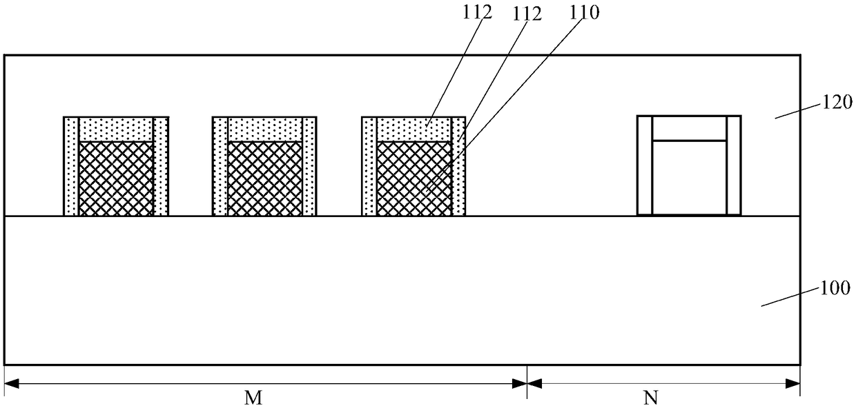
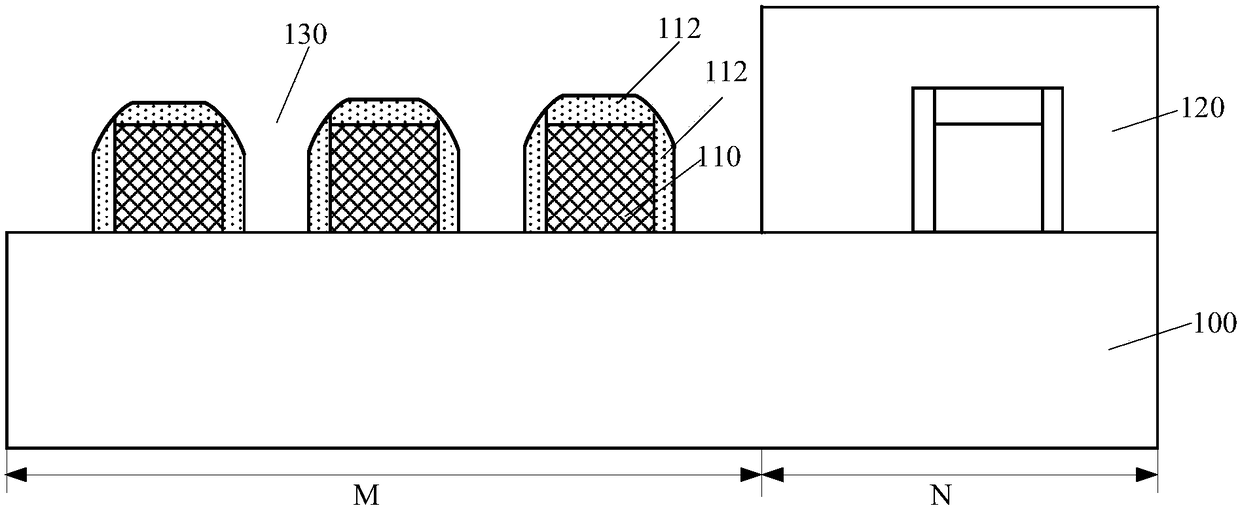
[0032] Figure 1 to Figure 2 It is a structural schematic diagram of a self-aligned etching process of a semiconductor device.

[0033] refer to figure 1 , provide a substrate 100, the substrate 100 includes a first region M and a second region N adjacent to the first region M; a gate structure and a dielectric layer 120 covering the gate structure are formed on the first region M of the substrate 100, the gate structure It includes a gate structure body 110 and a protective layer 112 located on the sidewall and top surface of the gate structure body 110 , and the dielectric layer 120 is also located on the second region N of the substrate 100 .

[0034] refer to figure 2 , forming a mask layer (not shown) on the dielectric layer 120 in the second region N; using the mask layer as a mask to etch and remove the dielectric layer 120 in the first region M, and forming ...


PUM


Abstract

The invention discloses a semiconductor device and a formation method thereof. The method comprises the following steps that: forming first grid electrode structure bodies on the first area of a substrate, first initial protection layers and first dielectric layers, wherein the first initial protection layers are positioned on the surfaces of the side walls and the top wall of each first grid electrode structure body, and each first dielectric layer covers each first initial protection layer; etching to remove parts of each first dielectric layer of the first area to enable a second dielectriclayer to be formed on each first dielectric layer of the first area, and enabling the first initial protection layer on the top of each first grid electrode structure body and parts of the first initial protection layer on the side walls of each grid electrode structure body to be exposed; carrying out an intermediate processing technology for at least one time until the second dielectric layer is removed, and enabling the first initial protection layers to form first protection layers positioned on the surfaces of the side walls and the top of the first grid electrode structure body, whereinthe intermediate processing technology comprises the following step of carrying out back etching on parts of the second dielectric layer of the first area after parts of the first initial protectionlayer on the top of the first grid electrode structure body are planarized. By use of the method, the performance of the semiconductor device is improved.

Description

technical field [0001] The invention relates to the field of semiconductor manufacturing, in particular to a semiconductor device and a forming method thereof. Background technique [0002] MOS (Metal-Oxide-Semiconductor) transistors are one of the most important components in modern integrated circuits. The basic structure of the MOS transistor includes: a semiconductor substrate; a gate structure located on the surface of the semiconductor substrate, and the gate structure includes: a gate dielectric layer located on the surface of the semiconductor substrate and a gate electrode layer located on the surface of the gate dielectric layer; The source and drain doped regions in the semiconductor substrate on both sides of the pole structure. [0003] The working principle of the MOS transistor is: a voltage is applied to the gate structure, and a switching signal is generated by adjusting the current in the channel at the bottom of the gate structure. [0004] However, the ...

Claims


Application Information

Patent Timeline
IPC IPC(8): H01L21/336H01L29/78
CPCH01L29/66795H01L29/785
Inventor 张城龙纪世良张海洋
Owner SEMICON MFG INT (SHANGHAI) CORP
Why Eureka
Try Eureka