Color micro display device and preparation method thereof
A technology of micro-display devices and micro-display chips, which is applied in the direction of electric solid-state devices, semiconductor devices, electrical components, etc., can solve problems such as crosstalk, and achieve the effect of solving the problem of light-emitting crosstalk
- Summary
- Abstract
- Description
- Claims
- Application Information
AI Technical Summary
Problems solved by technology
Method used
Image

Examples
Embodiment 1
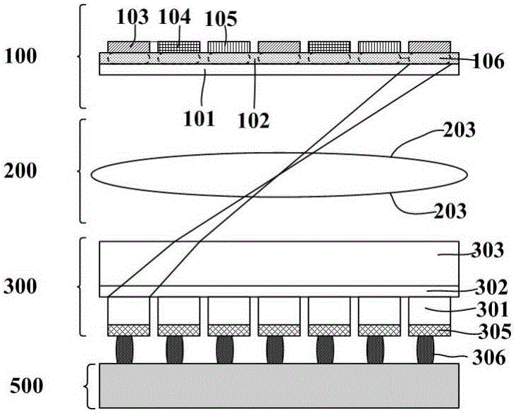
[0043] This embodiment is related to the preparation of a micro-pixel array wafer, and its preparation process is as follows:
[0044] 1) Depositing and growing a gallium nitride (GaN) LED epitaxial wafer on a polished sapphire substrate 303 .
[0045] 2) The LED micro-mesas array 301 is etched on the GaN LED epitaxial wafer, the etching depth is from the p-type GaN layer 308 to the quantum well 307 , and the etching ends at the n-type GaN layer 302 . The LED micro-mesas etched in this embodiment are rectangular, the area of the LED micro-mesas is 15um×15um, and the distance between adjacent micro-mesas is 5um. The shape of the micro-mesas of the array of the present invention is not limited to the rectangular shape, and the area of the mesas is set according to needs and process conditions, and is not limited to the given dimensions.
[0046] 3) Depositing a SiO2 passivation layer 304 on the surrounding sides of each LED micro-mesa on the epitaxial wafer, so as to cover ...
Embodiment 2
[0052] This embodiment is related to the preparation of the first type of imaging screen, the specific process is as follows:
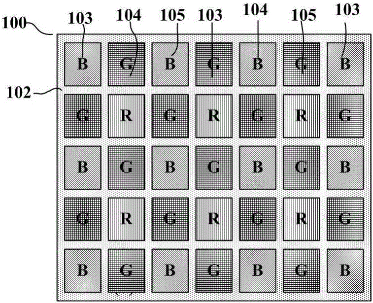
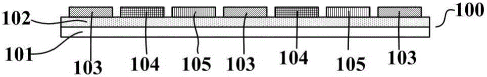
[0053] 1) Coating or depositing 20-30um white phosphor powder on the transparent substrate 102 to form a phosphor film 103 on the entire surface, see Figure 4 , 5 , the transparent substrate 102 may be a glass substrate or a plexiglass substrate or a sapphire substrate.
[0054] 2) Coating three primary color filter films arranged in an array on the above-mentioned white phosphor film 103 at set intervals, the three primary color filter films are red filter film 103, green filter film 104 and blue filter film 105. The color sorting is carried out in an array distribution according to the rule set in the figure. In this embodiment, the interval between adjacent filter films arranged in an array is 5um, and the area of each filter film is 15um×15um, thereby forming a filter film pixel array of three primary colors, thus forming the first type of co...
Embodiment 3
[0056] This embodiment is related to the preparation of the second type of imaging screen, the specific process is as follows:
[0057] 1) Coating or depositing 20-30um white phosphor powder on the transparent substrate 102 to form a white phosphor film 103, see Figure 6 , 7 , the transparent substrate 102 may be a glass substrate or a plexiglass substrate or a sapphire substrate.
[0058] 2) Coating photoresist on the surface of the above-mentioned white phosphor film 103, and forming a micro-surface phosphor film 402 arranged in an array through photolithography, development and etching, which is the same as the array arrangement of the above-mentioned three-color filter film , the size and spacing of the micro-facet phosphor film are determined by the size of the real image formed by the LED micro-pixel through the micro-lens. The size of the micro-facet phosphor film in this embodiment is 15um × 15um, and the distance between adjacent micro-facet phosphor films is 5um. ...
PUM
| Property | Measurement | Unit |
|---|---|---|
| Deposition thickness | aaaaa | aaaaa |
Abstract
Description
Claims
Application Information
 - R&D
- Intellectual Property
- Life Sciences
- Materials
- Tech Scout
- Unparalleled Data Quality
- Higher Quality Content
- 60% Fewer Hallucinations
Browse by: Latest US Patents, China's latest patents, Technical Efficacy Thesaurus, Application Domain, Technology Topic, Popular Technical Reports.
© 2025 PatSnap. All rights reserved.Legal|Privacy policy|Modern Slavery Act Transparency Statement|Sitemap|About US| Contact US: help@patsnap.com