3D Micro/Nano Measuring Probe

A measurement probe, micro-nano technology, applied in the direction of measuring devices, instruments, optical devices, etc., can solve the problems of low sensitivity and precision of strain gauge detection, easy fracture of silicon film structure, uneven stress distribution, etc., and achieve convenient manual adjustment , low cost, good stability

Active Publication Date: 2018-05-01
HEFEI UNIV OF TECH
View PDF6 Cites 0 Cited by
  • Summary
  • Abstract
  • Description
  • Claims
  • Application Information

AI Technical Summary

Problems solved by technology

When the end of the measuring rod is subjected to external force, the silicon membrane is deformed, and the displacement and force of the end of the measuring head are detected through the change of piezoresistance on the silicon membrane. The probe adopts 24 piezoresistive detection methods to improve Improve the detection sensitivity and reduce the influence of the probe on the temperature, but the thin film structure makes the stress distribution uneven, and the silicon film structure is relatively easy to break
The strain gauge-based three-dimensional micro-contact sensor head developed by the University of Eindhoven in the Netherlands. The strain gauge, the circuit and the elastic element are made into a whole through precipitation, plate making, etching and other processes. The force and displacement of the probe in all directions The change of the strain gauge is detected by the strain gauge installed on the sensitive beam. The volume is small, but the detection sensitivity and precision of the strain gauge are relatively low, and the probe adopts a triangular topology, which makes the decoupling complicated.
METAS, the Swiss Federal Bureau of Metrology and Testing, has developed an electromagnetic micro-contact probe. The probe has degrees of freedom in three directions. The detection in each direction is realized by inductance. The force measurement in the three directions is the same. The structure is mainly made of aluminum. The electromagnetic measuring head has a high measuring range, high lateral pick-up sensitivity and small contact force, but its structure is very complicated, difficult to install and adjust, and it adopts a triangular suspension structure, which makes decoupling very troublesome

Method used


Image

  • 3D Micro/Nano Measuring Probe
  • 3D Micro/Nano Measuring Probe
  • 3D Micro/Nano Measuring Probe

Examples


Embodiment Construction

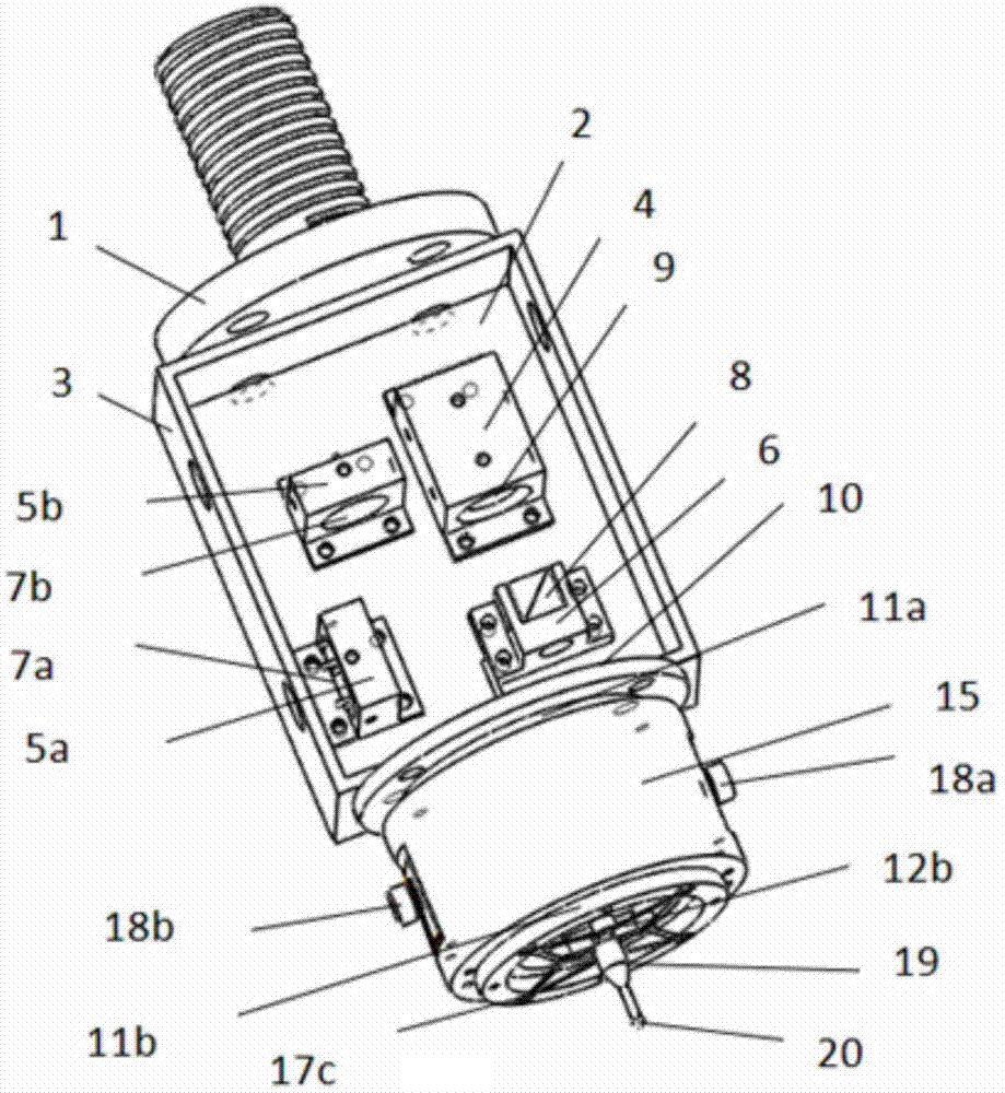
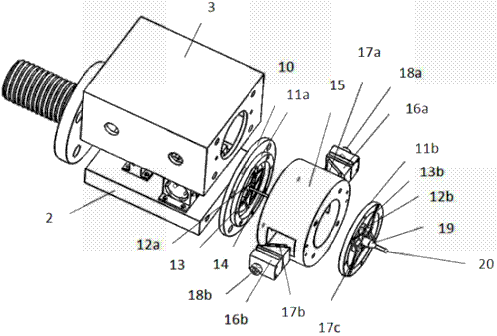
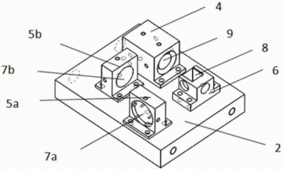
[0029] see figure 1 In this embodiment, the three-dimensional micro-nano measurement probe is fixedly connected to the probe unit and the internal measurement unit by means of a support.

[0030] see figure 2 , Figure 6 and Figure 7, the measuring head unit is fixed on the front end surface of the hollow cylinder 15 with the front end ring 11b, and the four front end "V" shaped reeds 13b are connected one by one with the vertices of the front "V" shaped reeds 13b. The arm ends of each cantilever of the sheet 12b, the two feet of the front end "V" shaped reed 13b are connected to the end face of the front end ring 11b; The central position of the front end cross suspension plate 12b is fixedly provided with a central plane reflector 17c, and a probe 19 is installed on the cross suspension plate 12b toward the outside of the hollow cylinder, and the front end of the probe 19 has a ruby ​​measuring ball 20; The end face of the tail part of the tube 15 is fixedly provided w...


PUM


Abstract

The invention discloses a high-precision wide-measuring-range three-dimensional micro-nano measuring probe. The high-precision wide-measuring-range three-dimensional micro-nano measuring probe is characterized in that a measuring probe unit and a measuring unit are fixedly connected through a support part, the measuring probe unit of the probe is provided with a two-layer suspension structure, a front-end suspension structure body is provided with a planar reflecting mirror and a measuring probe needle, and a rear-end suspension structure body is fixedly provided with a light blocking blade and connected with the front-end suspension structure body through a connecting probe rod; the measuring unit has a beam splitter prism used for splitting light source beams into reflected light and transmission light, the light intensity of the reflected light is changed due to Z-direction linkage of the light blocking blade, the reflected light irradiates a first four-quadrant detector, and the transmission light irradiates a second four-quadrant detector through reflection of three planar reflecting mirrors; displacement and two-dimensional angle measurement on the planar reflecting mirrors is achieved through detection signals output by the first four-quadrant detector and the second four-quadrant detector. The high-precision wide-measuring-range three-dimensional micro-nano measuring probe can achieve the detection effects of being high in precision and sensitivity, wide in measuring range, small in measuring force and high in stability.

Description

technical field [0001] The invention relates to the field of three-dimensional micro-nano measurement, more specifically, a high-precision and large-range three-dimensional micro-nano measuring probe applied to a nano-coordinate measuring machine, which can sense the three-dimensional shape of the surface of an object. Background technique [0002] With the rapid development of nanotechnology, all walks of life are competing to launch a technological revolution in the miniaturization of devices, and micro devices with sizes between millimeters and microns have come out one after another. Especially with the rapid development of MEMS (Micro-Electro-Mechanical System) device processing technology, various tiny devices with nanoscale as the standard have emerged. MEMS products such as micro-turbine, micro-needle array, gear-driven micro-motor, micro-lens, micro-nozzle and micro-gear. The geometric structure of these micro-devices is becoming more and more complex, and the geom...

Claims


Application Information

Patent Timeline
Patent Type & Authority Patents(China)
IPC IPC(8): G01B11/24
CPCG01B11/24
Inventor 李瑞君许鹏向萌范光照程真英
Owner HEFEI UNIV OF TECH
Why Eureka
Try Eureka