On-chip random access memory built-in self-testing method and device

A random access memory, built-in self-test technology, applied in the field of testing, can solve problems such as inflexibility and efficiency, and achieve the effect of saving testing time, increasing the number, and reducing testing steps

Active Publication Date: 2016-07-13
DATANG MICROELECTRONICS TECH CO LTD +1
View PDF4 Cites 15 Cited by
  • Summary
  • Abstract
  • Description
  • Claims
  • Application Information

AI Technical Summary

Problems solved by technology

However, the existing on-chip RAMBIST detection circuit only detects RAM physical fault defects functionally, and is not flexible and efficient enough

Method used


Image

  • On-chip random access memory built-in self-testing method and device
  • On-chip random access memory built-in self-testing method and device
  • On-chip random access memory built-in self-testing method and device

Examples


Embodiment Construction

[0030] In order to make the purpose, technical solution and advantages of the present invention more clear, the embodiments of the present invention will be described in detail below in conjunction with the accompanying drawings. It should be noted that, in the case of no conflict, the embodiments in the present application and the features in the embodiments can be combined arbitrarily with each other.

[0031] The steps shown in the flowcharts of the figures may be performed in a computer system, such as a set of computer-executable instructions. Also, although a logical order is shown in the flowcharts, in some cases the steps shown or described may be performed in an order different from that shown or described herein.

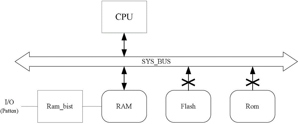
[0032] figure 1 It is a schematic diagram of the on-chip RAMBIST circuit structure in the embodiment of the present invention, such as figure 1 As shown, the RAMBIST module receives information through the I / O (input / output) interface, and communicates w...


PUM


Abstract

The embodiment of the invention provides an on-chip random access memory built-in self-testing (RAM BIST) method and device.The method includes the steps that a writing-in functional mode Pattern and a testing function Pattern are preset; when an RAM BIST module receives the writing-in function Pattern, the RAM BIST module is switched into an RAM writing-in program state, an instruction in the writing-in function Pattern is written in an RAM, a CPU maps a valuing address into a corresponding RAM, and the instruction is read according to the valuing address; when the RAM BIST module receives the testing function Pattern, based on a March LR algorithm, the instruction starts to be executed on the RAM for testing from a testing starting address, and a testing result is output.By means of the embodiment of the invention, the number of testing chips can be increased, detection time can be saved, detection steps can be reduced, and therefore chip testing cost is reduced, and testing efficiency is improved.

Description

technical field [0001] The embodiment of the present invention relates to the technical field of testing, in particular to a method and device for built-in self-testing of an on-chip random access memory supporting data writing. Background technique [0002] RAM (Random-Access Memory, Random Access Memory) is widely used in integrated circuit products due to its advantages of low power consumption and small silicon area overhead. With integrated circuit products, such as on-chip RAM capacity and quantity increasing, RAM failure will inevitably occur in the manufacturing process, and chips with failed memory units will cause unpredictable errors at the product level , leading to a surge in correction costs. Therefore, in the Wafer stage, high-coverage testing and screening of RAM has become a very important part of the entire life cycle of the chip, and how to quickly locate defective units through Wafer testing to improve detection coverage, thereby reducing test time and i...

Claims


Application Information

Patent Timeline
Patent Type & Authority Applications(China)
IPC IPC(8): G06F11/267G06F11/22
CPCG06F11/2268G06F11/2273G06F11/267
Inventor 王震张祥杉
Owner DATANG MICROELECTRONICS TECH CO LTD
Why Eureka
Try Eureka