Low Phase Noise RF Frequency Synthesis Circuit
A low phase noise, RF frequency technology, applied in the direction of electrical components, automatic power control, etc., can solve the problems of large output signal phase noise, large harmonic clutter, complex debugging, etc., to achieve low phase noise, harmonic clutter, etc. The effect of excellent performance and harmonic clutter characteristics
- Summary
- Abstract
- Description
- Claims
- Application Information
AI Technical Summary
Problems solved by technology
Method used
Image
Examples
Embodiment 1
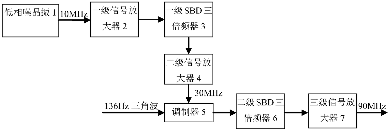
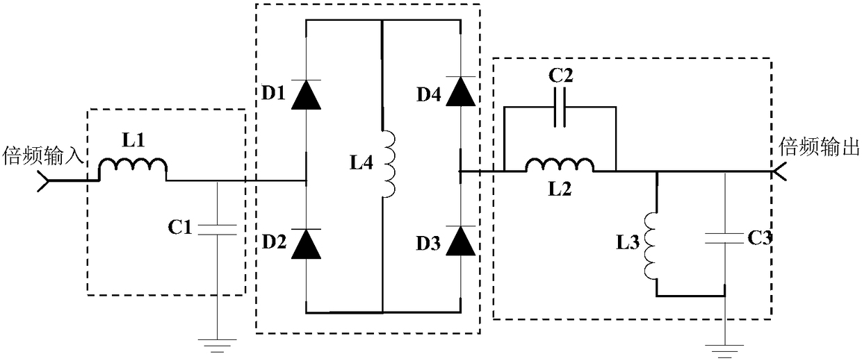
[0031] Such as figure 2 As shown, the low phase noise RF frequency synthesis circuit includes a low phase noise crystal oscillator 1 (10MHz low phase noise crystal oscillator is selected), the low phase noise crystal oscillator 1 is connected to the input terminal of the first-level signal amplifier 2, and the output terminal of the first-level signal amplifier 2 Connect with the input end of one-level SBD frequency tripler 3, the output end of one-level SBD frequency tripler 3 is connected with the input end of secondary signal amplifier 4, the output end of secondary signal amplifier 4 is connected with the first of modulator 5 One input terminal is connected, the second input terminal of modulator 5 is connected to triangular wave, the output terminal of modulator 5 is connected with the input terminal of secondary SBD frequency tripler 6, the output terminal of secondary SBD frequency tripler 6 is connected with three The input terminal of stage signal amplifier 7 is conn...
Embodiment 2
[0052] according to figure 2 It can be seen that the low phase noise RF frequency synthesis circuit includes a low phase noise crystal oscillator 1, a first-level signal amplifier 2, a first-level SBD tripler 3, a second-level signal amplifier 4, a modulator 5, and a second-level SBD tripler connected in sequence 6 and a three-stage signal amplifier 7. The specific parameters are as follows.
[0053] Low phase noise crystal oscillator 1 uses a 10MHz crystal oscillator with a phase noise lower than -150dBc / Hz@100Hz, and the output power is 5-10dBm.
[0054] Such as Figure 5 As shown, in the circuit of the first-stage signal amplifier 2. The bias resistor R1 is 500Ω, the resistor R2 is 10kΩ, and the resistor R3 is 10kΩ. The input coupling capacitor C9 is 200pF, and the output coupling capacitor C10 is 200pF. The inductance L8 of the band-stop network of the launch stage is 100nH, and the inductance C8 is 470pF. The inductance L7 of the collector frequency selection netwo...
PUM
 Abstract
Description
Claims
Application Information


