PCB board half hole forming process
A PCB board and hole forming technology, which is applied to the formation of electrical connections of printed components, printed circuits, electrical components, etc., can solve the problem of unstable deburring effect of half-holes, uncompetitive cost and delivery time, and prolonged half-hole milling time to avoid material offset deformation, save process steps, and reduce machining paths
- Summary
- Abstract
- Description
- Claims
- Application Information
AI Technical Summary
Problems solved by technology
Method used
Image

Examples
Embodiment 1
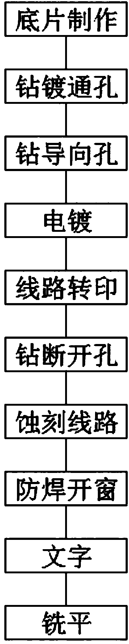
[0043] Such as figure 1 As shown, a PCB half-hole forming process, the steps include:
[0044] ① Production of film: Carry out CAM design of circuit film and solder mask film according to the original design drawing, in which the line width of the CAM design circuit is 10% wider than the original design drawing, and the diameter of the CAM design welding mask window is 20% larger than the original design drawing. At the same time, the image of the solder mask image designed by CAM compensates for the overlapping part of the line-solder mask that is larger than the range of the pad 42, such as Figure 8 ;
[0045] ②Drilling the plated through hole 2a: drill a plated through hole 2a with a diameter D on the boundary 1a between the removed area 11 and the reserved area 12 of the circuit board;
[0046] ③ Drill pilot hole 3a: drill out pilot hole 3a away from plated through hole 2a in circuit board 1 removal area 11, pilot hole 3a diameter D1=0.7D, as figure 2 ;
[0047] ④ El...
Embodiment 2
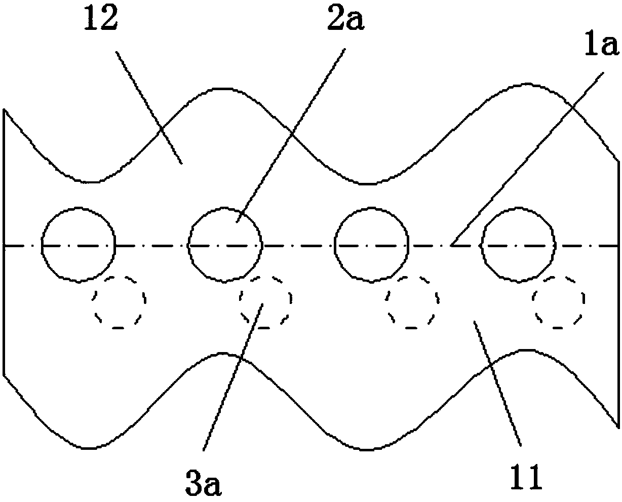
[0058]① Production of film: Carry out CAM design of line film and solder mask film according to the original design drawing, wherein the line width of the CAM design circuit is 20% wider than the original design drawing, and the diameter of the CAM design welding mask opening is 30% larger than the original design drawing. At the same time, the image of the solder mask image designed by CAM compensates for the overlapping part of the line-solder mask that is larger than the range of the pad 42, such as Figure 9 ;
[0059] ② Drilling: drill a plated through hole 2a with a diameter of D on the boundary 1a between the removed area 11 and the reserved area 12 of the circuit board, and drill a guide away from the plated through hole 2a in the removed area 12 of the circuit board 1 Hole 3a, guide hole 3a diameter D1=0.7D, as figure 2 ;
[0060] ③Electroplating: Copper film 4 is plated on the surface of the circuit board;
[0061] ④ Circuit transfer: Apply exposure ink on the ci...
Embodiment 3
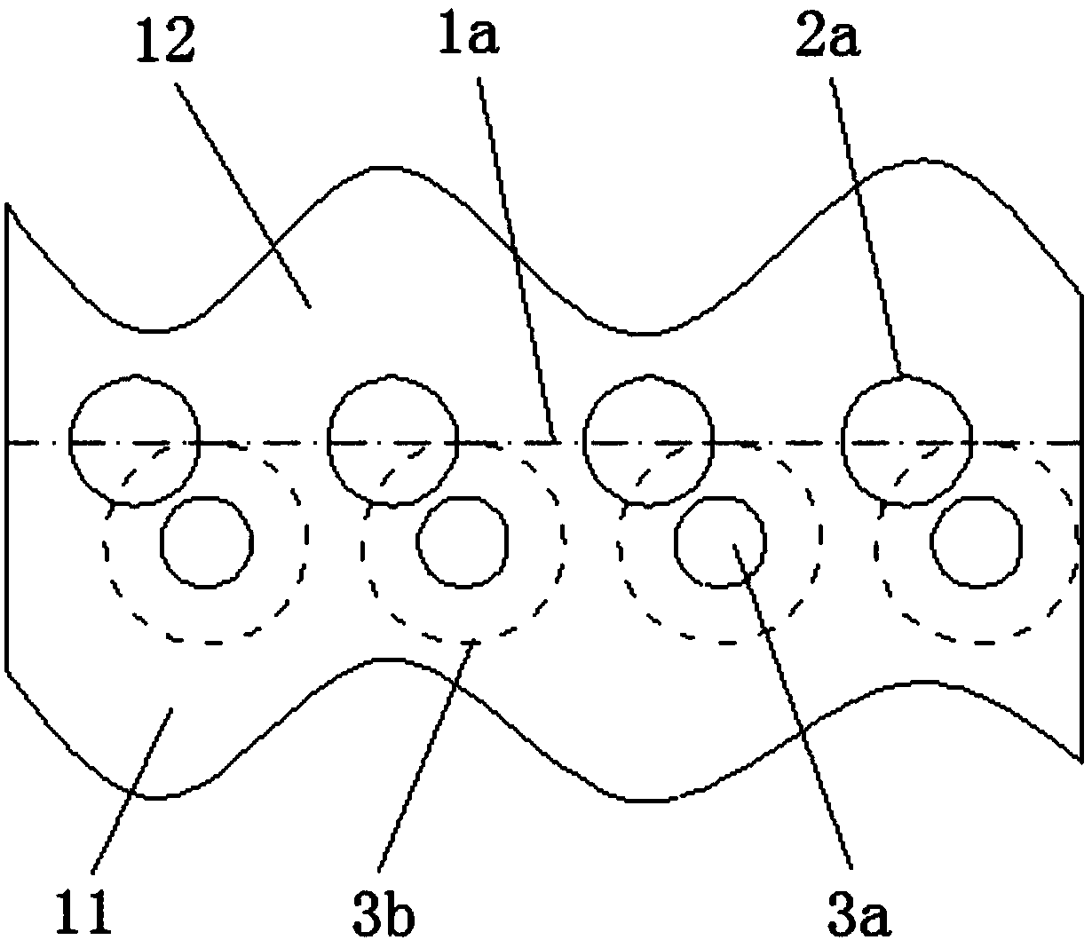
[0069] Such as Figure 6 As shown, the difference from Embodiment 2 is that the drill bit 71 for drilling plated through holes drills through the circuit board 1 , and then the drill bit 72 for drilling pilot holes drills through the circuit board 1 . Because the plated through hole 2a is a hole that actually needs to be reserved, and the guide hole 3a is a hole that will be eliminated, so the position accuracy of the plated through hole 2a is required to be higher, and it needs to be drilled out first. After the plated through-hole drill bit 71 drills through the circuit board 1 first, the circuit board 1 can be released from stress and returned to be flat, so that the circuit board 1 will not be broken due to excessive force at the same time when the pilot hole 3a is drilled.
PUM
 Abstract
Description
Claims
Application Information
 - R&D
- Intellectual Property
- Life Sciences
- Materials
- Tech Scout
- Unparalleled Data Quality
- Higher Quality Content
- 60% Fewer Hallucinations
Browse by: Latest US Patents, China's latest patents, Technical Efficacy Thesaurus, Application Domain, Technology Topic, Popular Technical Reports.
© 2025 PatSnap. All rights reserved.Legal|Privacy policy|Modern Slavery Act Transparency Statement|Sitemap|About US| Contact US: help@patsnap.com