BLOCK RAM (Random Access Memory) cascade structure of field programmable gate array FPGA

A cascade structure, SRAM18K technology, applied in the direction of instrumentation, electrical digital data processing, etc., can solve the problem of occupying programmable logic device wiring and logic resources, etc., to save peripheral wiring resources, small sequence loss, and improve the routing rate Effect

Inactive Publication Date: 2016-07-27
58TH RES INST OF CETC
View PDF4 Cites 4 Cited by
  • Summary
  • Abstract
  • Description
  • Claims
  • Application Information

AI Technical Summary

Problems solved by technology

[0004] When the user designs a storage unit BRAM that requires a large address depth and data width, the address depth and data width cascading function of mult

Method used


Image

  • BLOCK RAM (Random Access Memory) cascade structure of field programmable gate array FPGA
  • BLOCK RAM (Random Access Memory) cascade structure of field programmable gate array FPGA
  • BLOCK RAM (Random Access Memory) cascade structure of field programmable gate array FPGA

Examples


Embodiment Construction

[0032] The embodiments listed in the present invention are only used to help understand the present invention, and should not be interpreted as limiting the protection scope of the present invention. For those of ordinary skill in the art, they can also Improvements and modifications are made to the present invention, and these improvements and modifications also fall within the protection scope of the claims of the present invention.

[0033] In order to realize the memory unit RAM with the required address depth and data width, the software algorithm is simplified and the peripheral wiring resources are saved. The invention proposes a BLOCKRAM cascade structure of field programmable device FPGA.

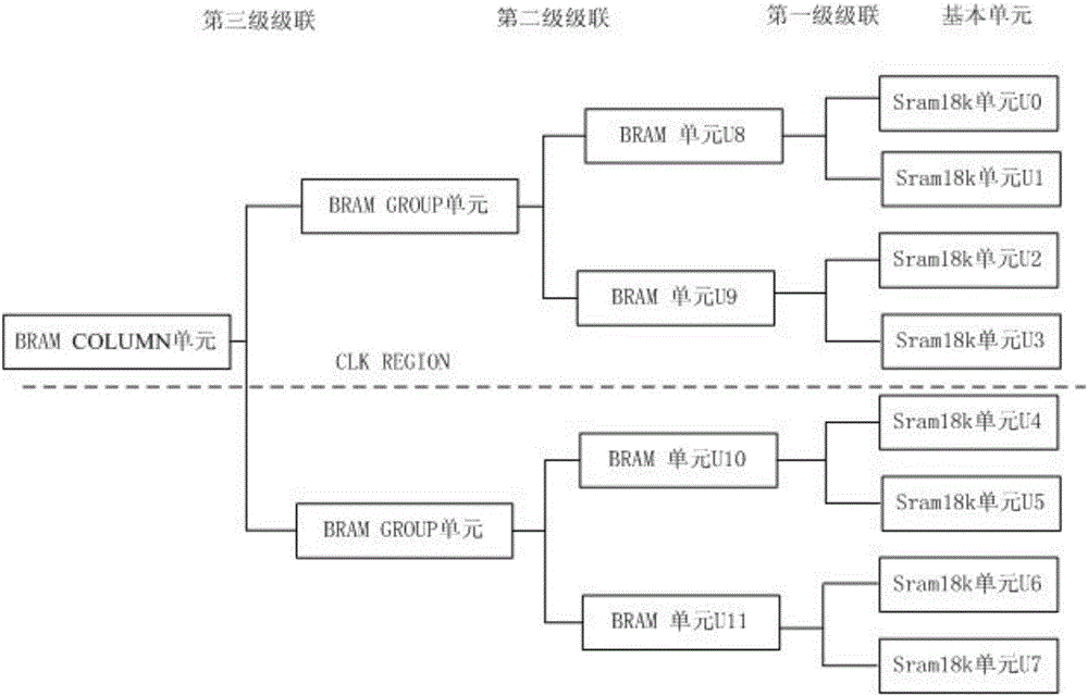
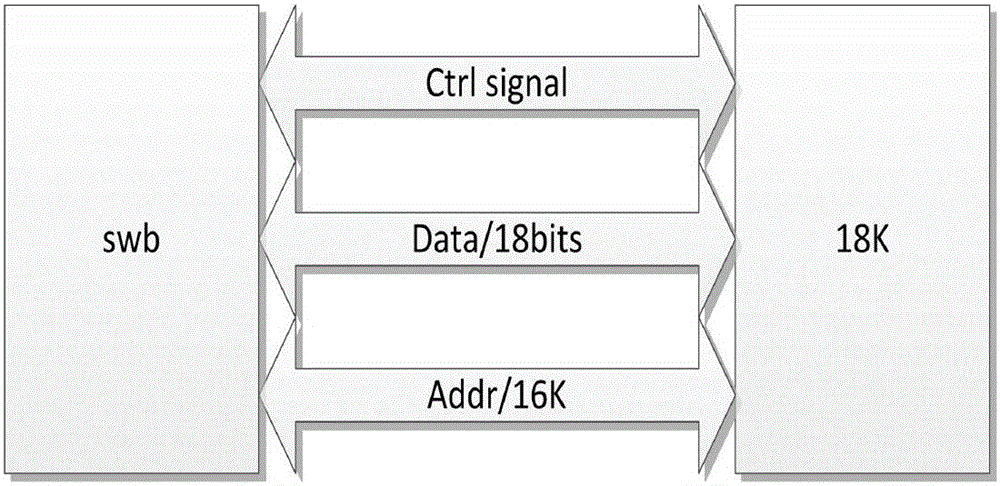
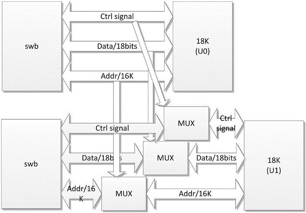
[0034] like figure 1As shown, it is the cascade structure supported by the 144KBLOCKRAM inside the field programmable device FPGA. It is described with 4 BLOCKRAM units U8, U9, U10, and U11 as an example, that is, there are 8 SRAM18K units U0, U1, U2, U3, U4, U5, U6, U7. The cas...


PUM


Abstract

The invention relates to a BLOCK RAM (Random Access Memory) cascade structure of a field programmable gate array FPGA. The BLOCK RAM cascade structure comprises a column of SRAM18K (Static Random Access Memory) units, wherein two adjacent SRAM18K units in one column of the SRAM18K units are in address cascade or data parallel connection through a first stage ASIC (Application Specific Integrated Circuit) cascade logic routing architecture, and one BLOCK RAM unit is formed, and the like, taking wiring of a CLK REGION in the FPGA as the limit, two adjacent BLOCK RAM units are cascaded and one BRAM GROUP unit is formed; and two adjacent BRAM GROUP units are cascaded to form one BRAM COLUMN unit, and a BLOCK RAM cascade structure with the required address depth and data width can be formed. The BLOCK RAM cascade structure of the field programmable gate array FPGA provided by the invention can realize a memory cell RAM with the required address depth and data width, simplify a software algorithm and save peripheral wiring resources.

Description

technical field [0001] The invention belongs to the technical field of programmable logic devices, and relates to a cascade structure, in particular to a BLOCKRAM cascade structure of a field programmable device FPGA. Background technique [0002] Field programmable device FPGA integrates programmable logic unit (CLB), digital signal processing (DSP), clock management, storage unit (BLOCKRAM), high-speed interface and other units. It has the characteristics of dual programming of software and hardware, and is a general-purpose platform system integrated chip. The RAM used to realize the storage function mainly includes two kinds of RAM: BLOCKRAM and distributed RAM (DistributedRAM). In the FPGA, the function generator (LUT) in the programmable logic unit (CLB) is configured as a synchronous RAM resource called DistributedRAM, which is mainly used for RAM requirements with small depth and small data bit width. And BLOCKRAM is mainly used in the construction of data high-spe...

Claims


Application Information

Patent Timeline
IPC IPC(8): G06F13/16
CPCG06F13/1668
Inventor 丛红艳闫华于宗光单悦尔胡凯
Owner 58TH RES INST OF CETC
Why Eureka
Try Eureka