Pixel unit, production method thereof, array substrate and display device

A pixel unit and array substrate technology, applied in the field of technical display, can solve the problems of affecting the display effect, limited light-emitting area, and affecting the light-emitting effect, so as to achieve the effects of improving the light-emitting effect, increasing the light-emitting area, and shortening the production time

Active Publication Date: 2016-07-27
BOE TECH GRP CO LTD +1
View PDF4 Cites 9 Cited by
  • Summary
  • Abstract
  • Description
  • Claims
  • Application Information

AI Technical Summary

Problems solved by technology

[0002] Organic light-emitting diode display device (OLED) is a new type of light-emitting technology, which uses stimulated radiation of organic matter to emit light. OLED drive methods are divided into active drive and passive drive. The active drive uses thin-film transistors (TFT) as The driving device, the pixel unit is driven by the corresponding TFT to form a TFT driving array, wherein the OLED driven by low-temperature polysilicon thin-film transistor (LTPS-TFT) 100 has faster electron transfer rate, smaller thin-film circuit area, higher resolution and structure The advantages of simplicity and high stability, the pixel unit of the low-temperature polysilicon thin-film transistor organic light-emitting diode (LTPS-TFTOLED) display device in the prior art such as figure 1 As shown, the pixel unit generally includes a low-temperature polysilicon thin film transistor as a driving thin film transistor 100, a planarization layer 200, a pixel definition layer 300, a pixel electrode 400, a light emitting layer 500, and a common electrode 600. The two sides of the light emitting layer 500 are directly When in contact with the pixel defining layer 300, the light emitted by the light emitting layer 500 will be scattered to the surrounding through the pixel defining layer 300, and will mix with the scattered light of other pixel units around it, seriously affecting the display effect. contact, the light-emitting area is limited, affecting the overall brightness
Additionally, if figure 1 The process flow of the pixel unit shown is generally polysilicon (Poly)-gate insulating layer (Gate1)-gate (Gate2)-interlayer deposition layer (ILD)-source, drain (SD)-planarization layer ( PLN)-pixel electrode (Anode)-pixel definition layer (PDL)-pad spacer (PS)-light-emitting layer evaporation (EL)-common electrode (Vcom), this process requires two processes to prepare flat layer via holes and The pixel defining layer 300 requires two sets of mask plates, the process is more complicated and the cost is higher, and the method of forming the pixel electrode 400 first and then forming the pixel defining layer 300 will make the pixel electrode material after the process of forming the pixel defining layer 300 Residues pollute the pixel electrode 400, thereby affecting the luminous effect. Therefore, there is an urgent need in the art for a pixel unit that can avoid color mixing and a method for preparing a pixel electrode that is simple in process, relatively low in cost, and does not affect the luminous effect.

Method used


Image

  • Pixel unit, production method thereof, array substrate and display device
  • Pixel unit, production method thereof, array substrate and display device
  • Pixel unit, production method thereof, array substrate and display device

Examples


Embodiment Construction

[0044] In order to make the object, technical solution and advantages of the present invention clearer, the present invention will be described in further detail below in conjunction with specific embodiments and with reference to the accompanying drawings.

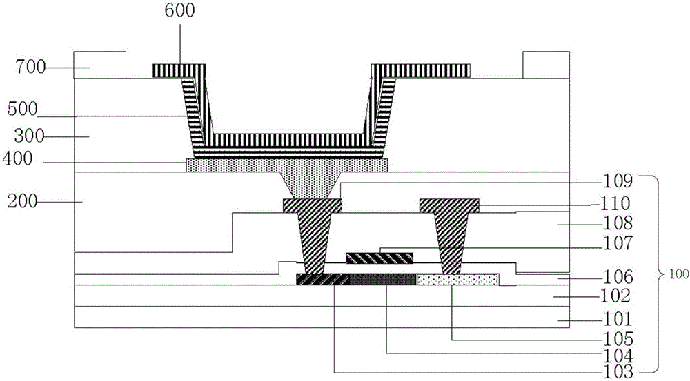
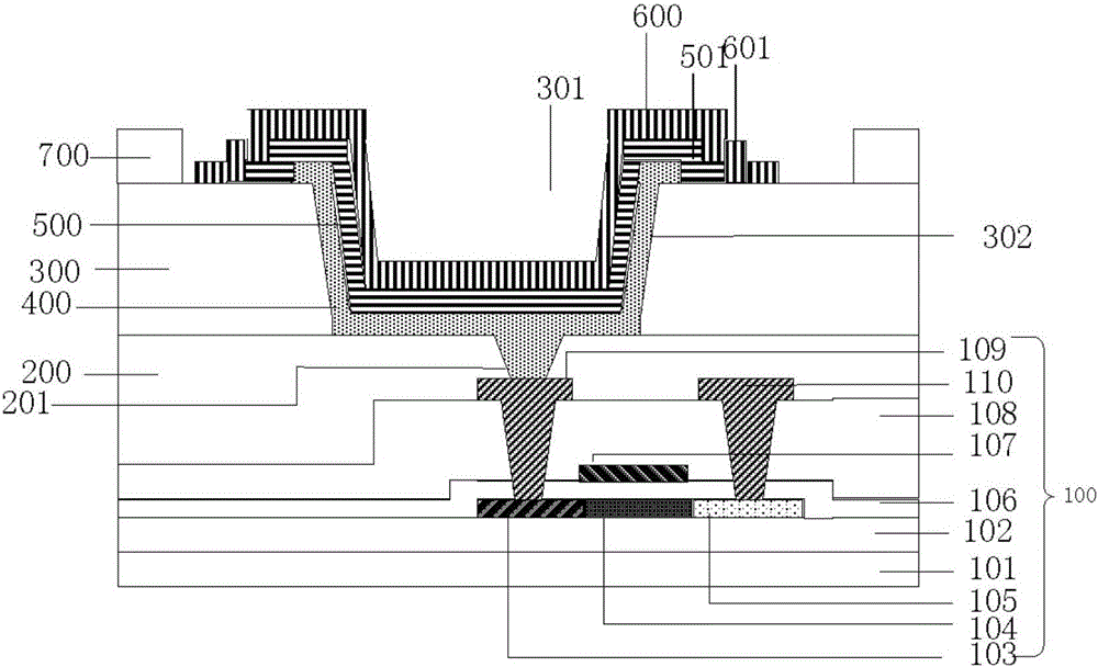
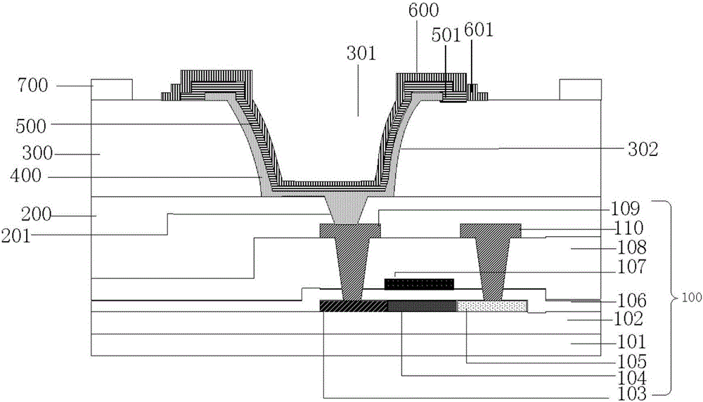
[0045] see figure 2 , figure 2 Shows the pixel unit of the first embodiment of the present invention, the pixel unit is formed on the driving thin film transistor, including: a planarization layer (PLN layer) 200, a pixel definition layer (PDL layer) 300, a pixel electrode 400, a light emitting layer 500 and common electrode 600,

[0046] Wherein, the driving thin film transistor may be a low-temperature polysilicon thin film transistor, including a substrate 101, a buffer layer 101 formed on the substrate 101, an output electrode 103-channel 104-input electrode 105 formed on the buffer layer 101, and an output electrode 103-channel 104-input electrode 105 formed on the buffer layer 101. Layer 102 and the gate insulat...


PUM


Abstract

The invention provides a pixel unit.The pixel unit comprises a pixel limiting layer, a pixel electrode, a light-emitting layer and a common electrode.The pixel electrode comprises a bottom face and a side face, and the side face extends to the top of the sidewall of a second via hole along the sidewall of the second via hole.The light-emitting layer is formed on the pixel electrode and covers the pixel limiting layer, and the common electrode is formed on the light-emitting layer, covers the light-emitting layer and extends along the top face of the pixel limiting layer.The pixel unit enables the light-emitting layer to scatter much less light to the surrounding, so that color mixing among pixel units is improved greatly, the problem of color mixing caused by light scattering is solved effectively, light-emitting area of the pixel unit is increased greatly, overall brightness is enhanced, mask film cost is reduced to enable cost of the whole technology to be reduced substantially, production capacity is improved and light-emitting effect is improved.

Description

technical field [0001] The present invention relates to the field of technical display technology, in particular to a pixel unit of an organic light emitting diode display device, a manufacturing method thereof, an array substrate and a display device. Background technique [0002] Organic light-emitting diode display device (OLED) is a new type of light-emitting technology, which uses stimulated radiation of organic matter to emit light. OLED drive methods are divided into active drive and passive drive. The active drive uses thin-film transistors (TFT) as The driving device, the pixel unit is driven by the corresponding TFT to form a TFT driving array, wherein the OLED driven by low-temperature polysilicon thin-film transistor (LTPS-TFT) 100 has faster electron transfer rate, smaller thin-film circuit area, higher resolution and structure The advantages of simplicity and high stability, the pixel unit of the low-temperature polysilicon thin-film transistor organic light-em...

Claims


Application Information

Patent Timeline
Patent Type & Authority Applications(China)
IPC IPC(8): H01L27/32H01L27/12G09F9/33
CPCG09F9/33H01L27/12H01L27/1214H10K59/00H10K59/1213H10K59/122H10K50/813H10K50/822H10K59/1201H10K59/805H10K50/805
Inventor 董向丹李坤代磊
Owner BOE TECH GRP CO LTD
Why Eureka
Try Eureka