A np-type single-photon avalanche diode based on cmos image sensor technology
A single-photon avalanche and image sensor technology, applied in semiconductor devices, electrical components, circuits, etc., can solve problems such as limitations and poor noise characteristics, and achieve the effects of enhancing response, improving noise characteristics, and reducing dark counts
- Summary
- Abstract
- Description
- Claims
- Application Information
AI Technical Summary
Problems solved by technology
Method used
Image
Examples
Embodiment Construction
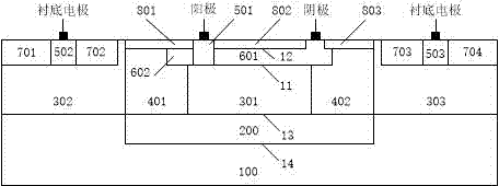
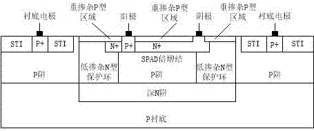
[0019] figure 1 It is an NP-type single-photon avalanche diode (SPAD) based on CMOS image sensor technology provided by the present invention, and its basic structure includes: a deep N well (200) is arranged above a P-type silicon substrate (100); a P well (301 ) is formed above and in contact with the deep N well (200); lightly doped guard rings (401, 402) are provided around the P well (301); N+ regions (601, 602) are formed in Above the P well (301) and overlaps with the lightly doped guard rings (401, 402) to a certain extent; N+ regions (601, 602) and lightly doped guard rings (401, 402) are provided with heavy doping Doped P-type regions (801, 802, 803), covering the entire surface of (601, 602) and (401, 402) except for the cathode and anode contacts; lightly doped guard rings around (401, 402) There are P wells (302, 303), and the P well region (302, 303) leads to the substrate electrode through the P+ region (502, 503); the heavily doped P type region (801, 802, 803...
PUM
 Abstract
Description
Claims
Application Information


