Optical semiconductor, method for producing same, surface treatment agent for silver, and light-emitting device

A technology for optical semiconductor devices and light-emitting devices, which is applied in the field of silver surface treatment agents and light-emitting devices, and can solve the problems of black, chemical instability of silver and silver alloys, etc.

Inactive Publication Date: 2016-07-27
HITACHI CHEM CO LTD
View PDF8 Cites 4 Cited by
  • Summary
  • Abstract
  • Description
  • Claims
  • Application Information

AI Technical Summary

Problems solved by technology

[0006] However, since silver and silver alloys are very unstable chemically, they are easy to react with oxygen, moisture, hydrogen sulfide, sulfurous acid gas, etc. black disadvantage

Method used


Image

  • Optical semiconductor, method for producing same, surface treatment agent for silver, and light-emitting device
  • Optical semiconductor, method for producing same, surface treatment agent for silver, and light-emitting device
  • Optical semiconductor, method for producing same, surface treatment agent for silver, and light-emitting device

Examples


no. 1 Embodiment approach

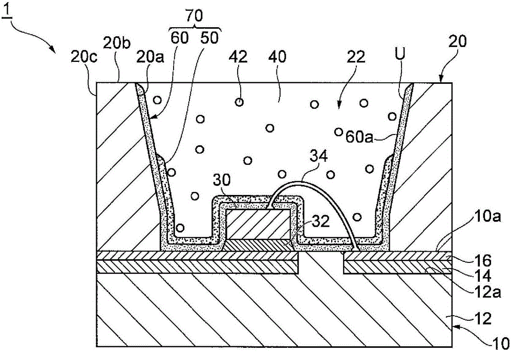
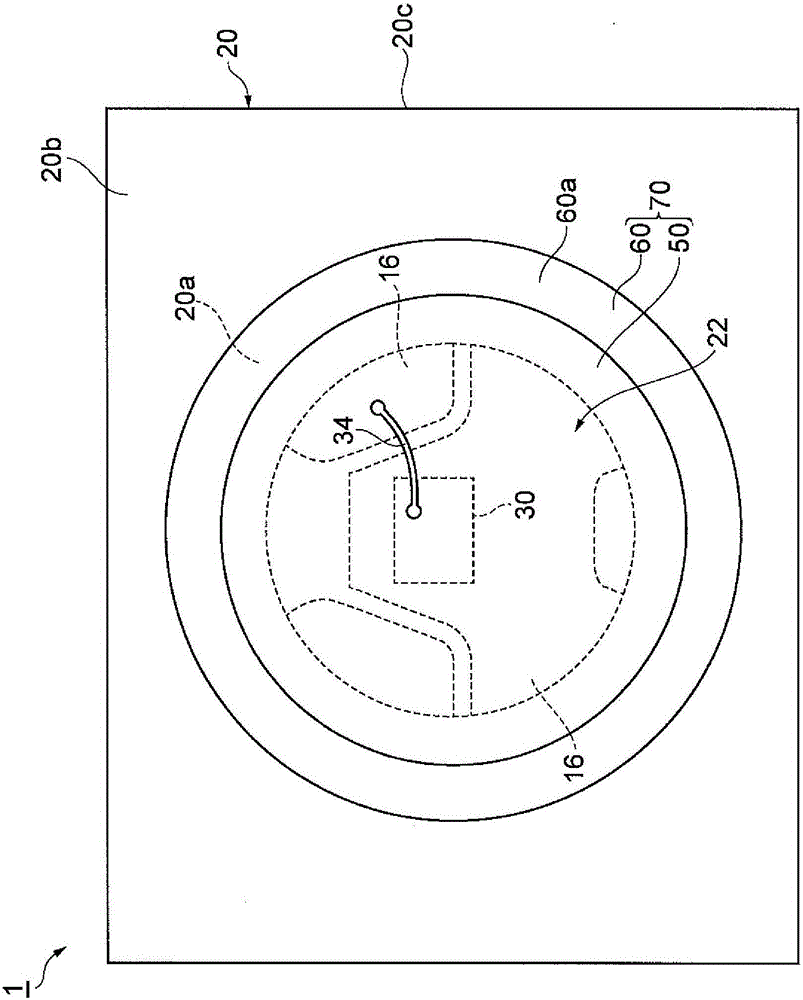
[0105] figure 1 It is a sectional view of the optical semiconductor device of the first embodiment. figure 2 for figure 1 A top view of the optical semiconductor device shown. Such as figure 1 and figure 2 As shown, the optical semiconductor device 1 of the embodiment is generally classified as "surface mount type". This optical semiconductor device 1 includes a substrate 10, a blue light-emitting diode 30 bonded to the surface of the substrate 10, a reflector 20 provided on the surface of the substrate 10 so as to surround the blue light-emitting diode 30, and a blue light-emitting diode 30 filled in the reflector 20. The transparent sealing part 40 which seals the light emitting diode 30, and the anti-silver sulfide film 70 which coats the silver-plated layer 16. in addition, figure 2 The illustration of the transparent sealing part 40 is omitted in .

[0106] In the substrate 10 , a copper-plated plate 14 is wired on the surface of an insulating base 12 , and a si...

no. 2 Embodiment approach

[0134] Next, a second embodiment will be described. The second embodiment is basically the same as the first embodiment, and only the formation position of the gas barrier layer is different from the first embodiment. Therefore, in the following description, only the points different from those of the first embodiment will be described, and the same description as that of the first embodiment will be omitted.

[0135] Image 6 It is a cross-sectional view of the optical semiconductor device of the second embodiment. Such as Image 6 As shown, the optical semiconductor device 2 of the second embodiment includes a silver sulfide preventing film 72 instead of the silver sulfide preventing film 70 of the first embodiment.

[0136] The silver sulfide prevention film 72 includes a gas barrier layer 52 and an undercoat layer 60 . The gas barrier layer 52 is basically the same as the gas barrier layer 50 , but differs from the gas barrier layer 50 in that the light reflection surf...

no. 3 Embodiment approach

[0140] Next, a third embodiment will be described. The third embodiment is basically the same as the first embodiment, and only the formation positions of the undercoat layer and the gas barrier layer are different from the first embodiment. Therefore, in the following description, only the points different from those of the first embodiment will be described, and the same description as that of the first embodiment will be omitted.

[0141] Figure 8 It is a cross-sectional view of the optical semiconductor device of the third embodiment. Such as Figure 8 As shown, the optical semiconductor device 3 of the third embodiment includes a silver sulfide preventing film 73 instead of the silver sulfide preventing film 70 of the first embodiment.

[0142] The silver sulfide preventing film 73 includes an undercoat layer 63 and a gas barrier layer 53 .

[0143]The undercoat layer 63 is basically the same as the undercoat layer 60, but differs from the undercoat layer 60 in that ...


PUM


Abstract

An optical semiconductor device according to one mode of the present invention is provided with a substrate in which a silver-plating layer is formed on a surface, a light-emission diode which is bonded to the silver-plating layer, a light reflection part which forms an inner space for housing the light-emission diode by means of light reflection surfaces surrounding the light-emission diode, a silver sulfurization prevention film which covers the silver-plated layer, and a transparent sealing part which seals the light-emission diode by being filled into the inner space, wherein: the silver sulfurization prevention film has a gas barrier layer exhibiting gas-barrier properties due to clay, and a primer layer provided to the lower layer of the gas barrier layer and exhibiting adhesive properties; and the transparent sealing part comes into contact with the primer layer.

Description

technical field [0001] The present invention relates to an optical semiconductor device to which a light emitting diode is bonded, a method for producing the same, a surface treatment agent for silver, and a light emitting device. [0002] The present invention relates to a surface treatment agent for silver, and more specifically to a surface treatment agent for preventing discoloration (corrosion) of various silver or silver alloys, especially for preventing the use of A surface treatment agent for discoloration (corrosion) of silver or silver alloys, especially the silver vapor-deposited surface. [0003] The present invention relates to a light-emitting device, and more specifically, to a light-emitting device including a substrate having silver or a silver alloy and a light-emitting diode. Background technique [0004] A device disclosed in Patent Document 1 is known as an optical semiconductor device on which an LED (light emitting diode: Light Emitting Diode) is moun...

Claims


Application Information

Patent Timeline
Patent Type & Authority Applications(China)
IPC IPC(8): H01L33/52H01L33/62
CPCH01L33/60H01L33/44H01L33/52H01L33/62H01L2224/45144H01L2224/48091H01L2224/48464H01L2224/73265H01L2224/8592H01L2924/00014H01L2924/00
Inventor 山浦格东内智子稻田麻希后藤泰史鲤渊滋高根信明
Owner HITACHI CHEM CO LTD
Why Eureka
Try Eureka