

OLED array substrate, manufacturing method thereof, display panel and display device
A technology of array substrates and substrates, which is applied in semiconductor/solid-state device manufacturing, semiconductor devices, electrical components, etc., and can solve the problems of multiple preparation processes of reflective layers and increased reflectivity
- Summary
- Abstract
- Description
- Claims
- Application Information
AI Technical Summary
Problems solved by technology
Method used
Image

Examples
Embodiment 1
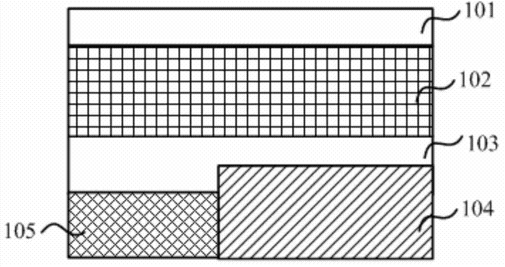
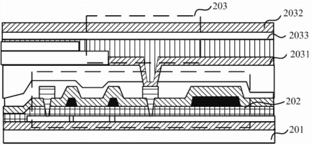
[0021] Such as figure 2 As shown, it is an OLED array substrate provided in Embodiment 1 of the present invention. The OLED array substrate includes: a substrate 201, a TFT array 202 located on the substrate 201, a plurality of OLED pixel units 203, and any OLED pixel unit 203 includes:
[0022] The first electrode 2031, the second electrode 2032, and the light emitting structure layer 2033 between the first electrode 2031 and the second electrode 2032, wherein the first electrode 2031 is closer to the Substrate 201.
[0023] In the embodiment of the present invention, the first electrode 2031 is a film layer formed by doping a dopant substance and graphene at a set molar ratio, wherein the dopant substance is a simple metal substance.
[0024] Preferably, the metal element is any one of silver, titanium, vanadium, iron, aluminum, zinc, tin, copper, gold or platinum.
[0025] In the embodiment of the present invention, since the structure of the array substrate involved is...
Embodiment 2
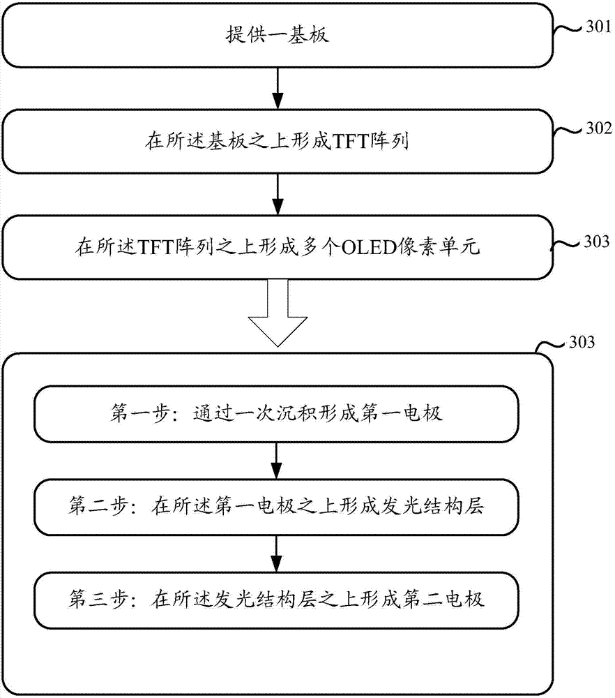
[0032] combine image 3 As shown, the method for preparing the OLED array substrate provided in the second embodiment of the present invention specifically includes the following steps:
[0033] Step 301: Provide a substrate.
[0034] The substrate may be a rigid substrate or a flexible substrate, and the present invention does not specifically limit the material of the substrate.
[0035] Step 302: forming a TFT array on the substrate.
[0036]After step 301, a thin film transistor array substrate, ie a TFT array, is formed on the substrate. Wherein, the TFT array includes: an active layer, a gate, a gate insulating layer, a source, a drain, a passivation layer and other structures, and the above structure is based on the film structure technology in the prior art (deposition, photolithography, etc.) process) are sequentially formed, and may be a top-gate structure or a bottom-gate structure.
[0037] Step 303: forming a plurality of OLED pixel units on the TFT array. Sp...
Embodiment 3
[0047] Based on the OLED array substrate provided by the embodiment of the present invention, Embodiment 3 of the present invention also proposes a display panel. The display panel includes the OLED array substrate described in Embodiment 1, and also includes a packaging cover plate and the like that are arranged opposite to the OLED array substrate in the prior art.
[0048] In addition, an embodiment of the present invention also provides a display device, including the display panel described in Embodiment 3 and other display device units in the prior art, such as a driving module, a polarizer, and the like.
PUM
| Property | Measurement | Unit |
|---|---|---|
| Thickness | aaaaa | aaaaa |
Abstract
Description
Claims
Application Information