Semiconductor structure and formation method thereof

A semiconductor and plasma technology, applied in the fields of semiconductor devices, semiconductor/solid-state device manufacturing, electrical components, etc., can solve the problems of unstable performance, poor transistor morphology, and increased process difficulty of high-K metal gate transistors. Reliable performance, good appearance, dense interior

Active Publication Date: 2016-08-03
SEMICON MFG INT (SHANGHAI) CORP
View PDF6 Cites 4 Cited by
  • Summary
  • Abstract
  • Description
  • Claims
  • Application Information

AI Technical Summary

Problems solved by technology

[0005] However, with the continuous shrinking of semiconductor process nodes, the size of the formed high-k metal gate transistors is continuously shrinking, which leads to an increase in the process difficulty of manufacturing high-k metal gate transistors, and the formed transistors have poor morphology and unstable performance.

Method used


Image

  • Semiconductor structure and formation method thereof
  • Semiconductor structure and formation method thereof
  • Semiconductor structure and formation method thereof

Examples


Embodiment Construction

[0032] As mentioned in the background art, the high-K metal gate transistors formed in the prior art have poor morphology and unstable performance.

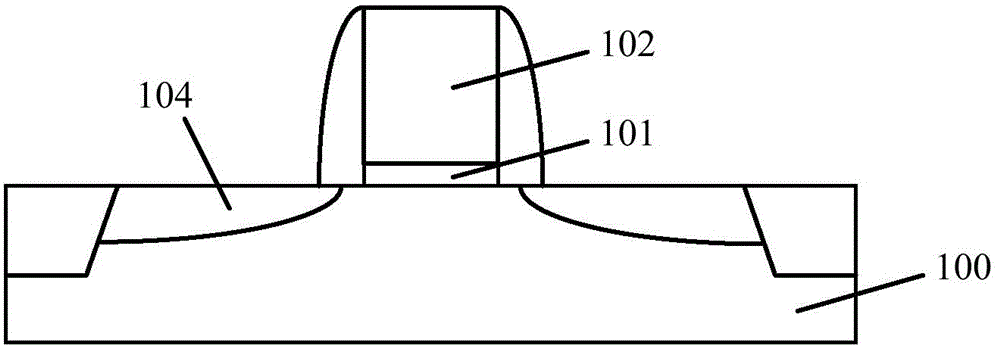
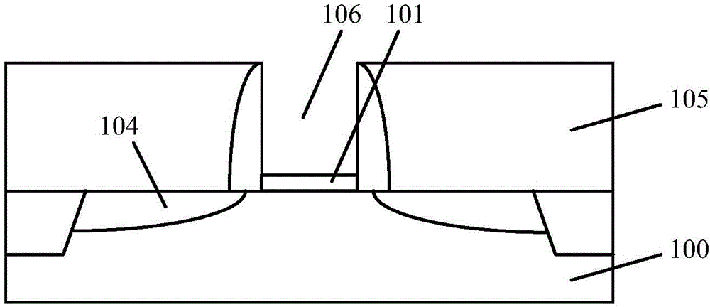
[0033] After research, it is found that the high-K metal gate transistor needs to be formed by a gate last process. Figure 1 to Figure 4 It is a schematic cross-sectional structure diagram of a process of forming a high-K metal gate transistor by using a gate-last process according to an embodiment of the present invention.

[0034] Please refer to figure 1 , providing a substrate 100; forming a gate dielectric layer 101 on the surface of the substrate 100, and a dummy gate layer 102 located on the surface of the gate dielectric layer 101; wall; forming a source region and a drain region 104 in the substrate 100 on both sides of the sidewall and the dummy gate layer 102 .

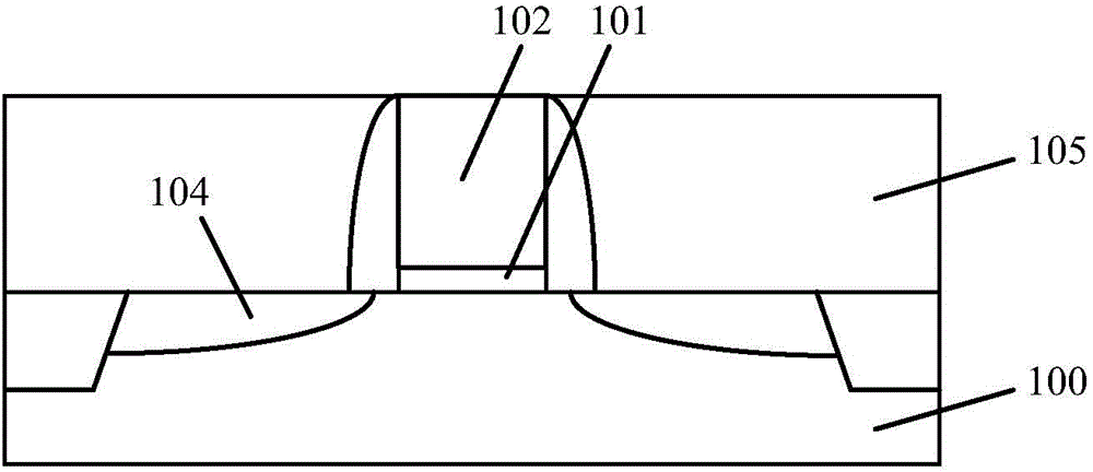
[0035] Please refer to figure 2 , forming a dielectric layer 105 on the surface of the substrate 100 , the surface of the dielectric layer 105 is flush w...


PUM


Abstract

The invention relates to a semiconductor structure and a formation method thereof. The formation method comprises the steps of providing a substrate, wherein the surface of the substrate is provided with a pseudo gate dielectric film, and the surface of the pseudo gate dielectric film is provided with a pseudo gate film; forming a mask layer at part of the surface of the pseudo gate film, carrying out a first etching process on the pseudo gate film by taking the mask layer as a mask so as to form a first trench in the pseudo gate film, wherein the side wall of the first trench is vertical with the surface of the substrate, carrying out a second etching process on the pseudo gate film at the bottom of the first trench until the surface of the pseudo dielectric film is exposed, forming a second trench at the bottom of the first trench, forming a pseudo gate layer adjacent to the left pseudo gate film between the first trench and the second trench, wherein the top of the second trench is less than the bottom of the second trench in size, and the angle between the side wall of the second trench and the bottom surface of the second trench is an acute angle, and carrying out a third etching process on the exposed pseudo gate dielectric film until the surface of the substrate is exposed so as to form a pseudo gate dielectric layer. The formed semiconductor structure is good in appearance and improved in performance.

Description

technical field [0001] The invention relates to the technical field of semiconductor manufacturing, in particular to a semiconductor structure and a forming method thereof. Background technique [0002] With the rapid development of integrated circuit manufacturing technology, the size of semiconductor devices in integrated circuits, especially MOS (Metal Oxide Semiconductor, metal-oxide-semiconductor) devices, is continuously reduced to meet the miniaturization and integration of integrated circuit development. Requirements, and transistor devices are one of the important components of MOS devices. [0003] For transistor devices, as the size of the transistor continues to shrink, the gate dielectric layer formed of silicon oxide or silicon oxynitride material in the prior art cannot meet the performance requirements of the transistor. In particular, transistors formed with silicon oxide or silicon oxynitride as the gate dielectric layer are prone to a series of problems s...

Claims


Application Information

Patent Timeline
Patent Type & Authority Applications(China)
IPC IPC(8): H01L21/28H01L21/336H01L29/423H01L29/78
Inventor 韩秋华
Owner SEMICON MFG INT (SHANGHAI) CORP
Why Eureka
Try Eureka