

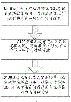
Semiconductor package method, semiconductor package piece, and method for manufacturing dynamic random access memory
A dynamic random access and packaging method technology, which is applied in semiconductor/solid-state device manufacturing, semiconductor devices, semiconductor/solid-state device components, etc., can solve the problem of increasing DRAM manufacturing, packaging costs, memory wafer structure accuracy, and reliable electrical performance. It can achieve the effect of expanding read and write speed, reducing size, and high transmission rate
- Summary
- Abstract
- Description
- Claims
- Application Information
AI Technical Summary
Problems solved by technology
Method used
Image

Examples
Embodiment Construction
[0040] In the following description, numerous specific details are set forth in order to provide a thorough understanding of the present invention. However, the present invention can be implemented in many other ways different from those described here, and those skilled in the art can make similar extensions without violating the connotation of the present invention, so the present invention is not limited by the specific implementations disclosed below.
[0041] Secondly, the present invention is described in detail using schematic diagrams. When describing the embodiments of the present invention in detail, it is used as an example for convenience of explanation. The schematic diagrams are only examples, which should not limit the protection scope of the present invention.
[0042] In the drawings, the proportions of shapes of elements may be exaggerated or reduced for clarity, and corresponding numerals refer to corresponding elements throughout. It will also be understood...
PUM
 Abstract
Description
Claims
Application Information