

Solder material and electronic component
A technology of electronic parts and solder, applied in welding/cutting media/materials, electrical components, welding media, etc., can solve problems such as unsuitable sealing materials, and achieve the effect of suppressing insufficient melting
Inactive Publication Date: 2016-08-10
NIHON DEMPA KOGYO CO LTD
View PDF9 Cites 4 Cited by
- Summary
- Abstract
- Description
- Claims
- Application Information
AI Technical Summary
Problems solved by technology
However, Bi has the property of volume expansion at normal temperature, and is not suitable as a sealing material for hermetically sealing the gap of a container.
Method used
View moreImage
Smart ImageViewing Examples

Examples
Embodiment 1
[0083] Sn is set to 38.0 mass%, Sb is set to 36.0 mass%, Ag is set to 15.0 mass%, Cu is set to 5.0 mass%, and In is set to 6.0 mass%. The solder material is produced by the well-known production method of the solder material shown.
Embodiment 2~ Embodiment 27
[0085] A solder material was produced in the same manner as in Example 1 except that the composition ratio of the solder material was set as shown in Table 1 below.
Embodiment 1-2
[0120] The following solder material was used as Example 1-2, that is, in the solder shown in Example 1, 0.01% by mass of the material in the mixed solder material was replaced with 0.005% by mass of Si and 0.005% by mass of Ti.
Login to View More PUM
| Property | Measurement | Unit |
|---|---|---|
| melting point | aaaaa | aaaaa |
| melting point | aaaaa | aaaaa |
| particle diameter | aaaaa | aaaaa |
Abstract
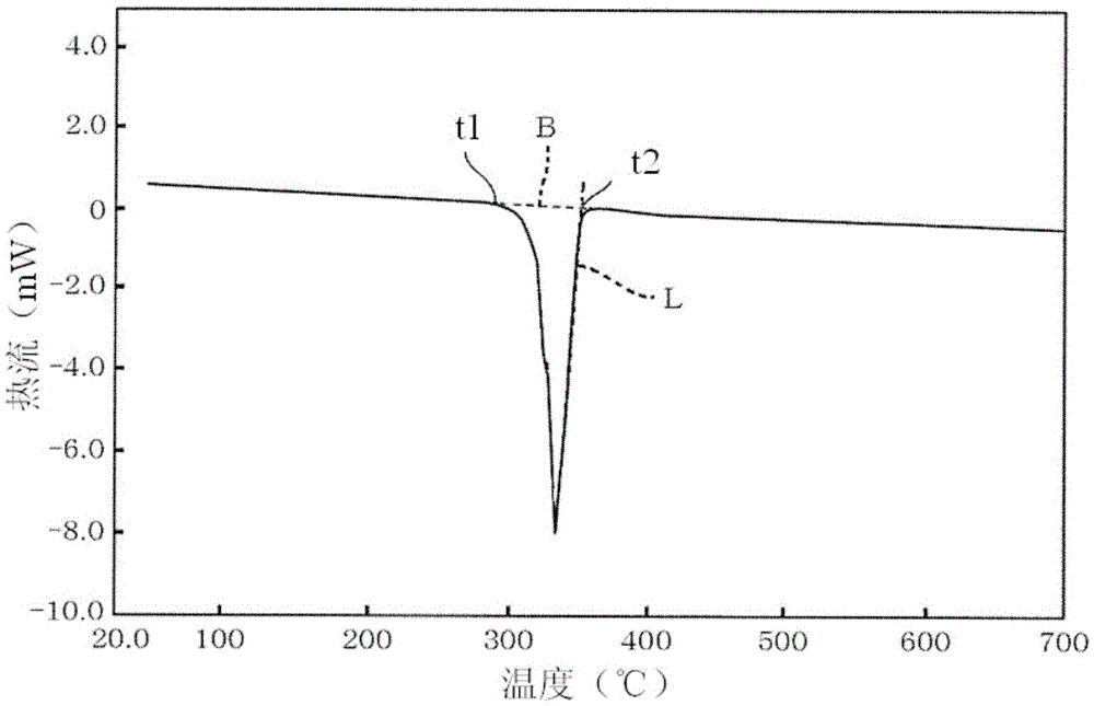
The invention provides a solder material and electronic component. The solder material includes an alloy of at least five elements including Sn, Cu, Sb, and In, and 20 mass % or less of Ag. The solidus temperature of the solder material is higher than 290 DEG C, the liquidus temperature of the solder material is 379 DEG C or less and is higher than the solidus temperature, and the temperature difference between the liquidus temperature and the solidus temperature is 70 DEG C or less. The melting temperature of solder material is reduced therefore. In the temperature range when the solder material is installed on a substrate and refluxed, the solder material is difficult to melt. The phenomenon that the solder material is not melted sufficiently, or the solder material is melted when parts are installed on the substrate is avoided.
Description
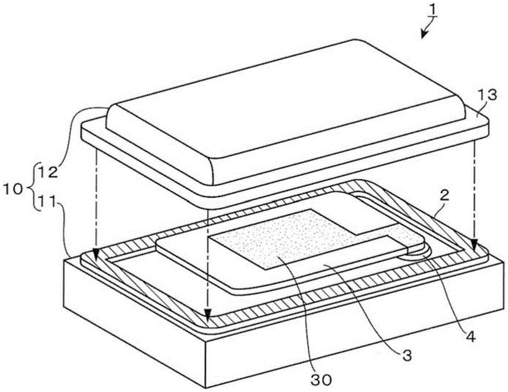
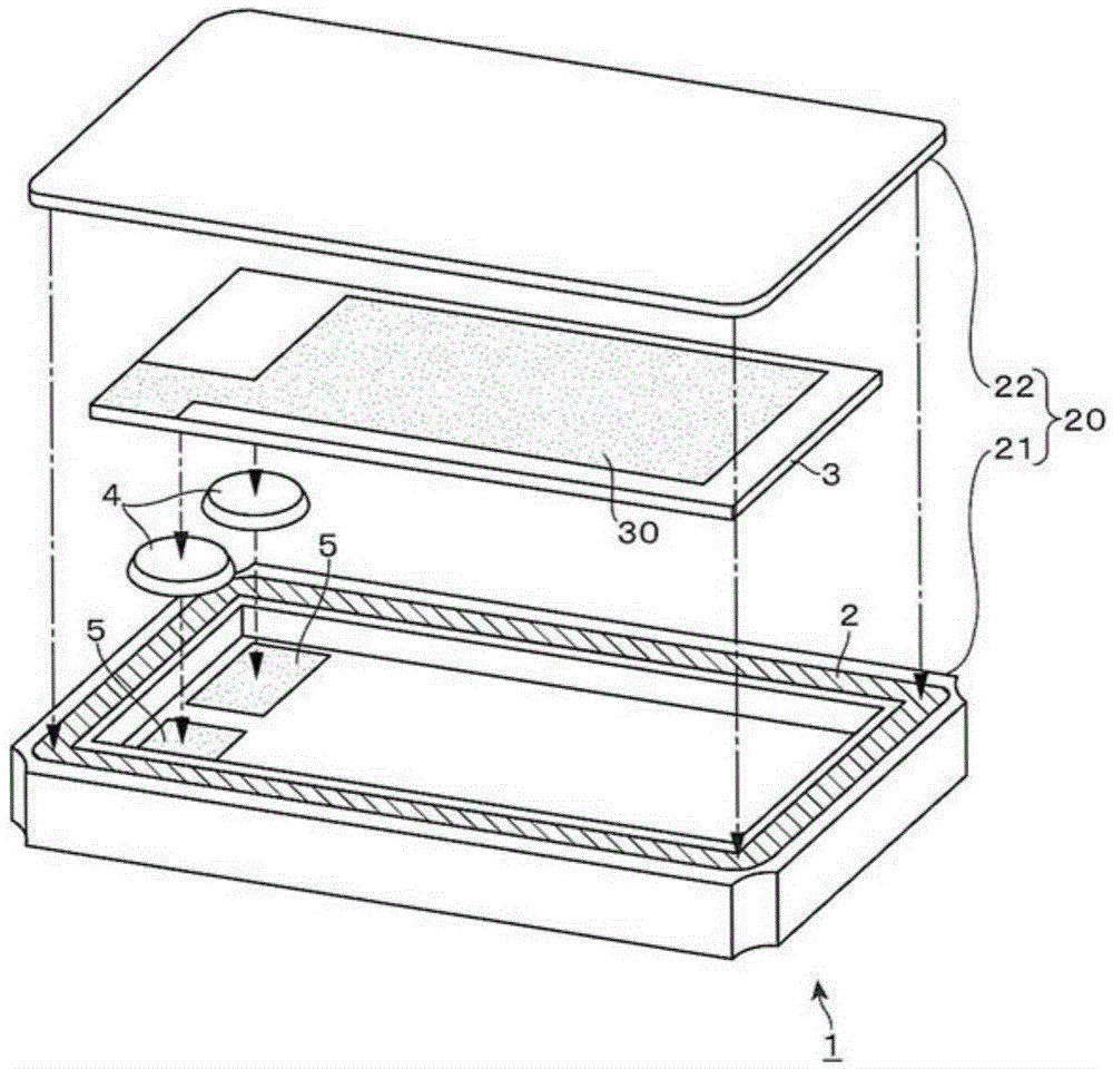
technical field [0001] The invention relates to a solder material and an electronic component mounted on a substrate using the solder material. Background technique [0002] For example, small electronic components such as surface acoustic wave devices and quartz resonators are housed in small containers to form surface mount components, and are mounted on substrates such as wiring boards. For example, at this time, a solder material is used as a sealing material for airtightly sealing a container of a surface mount component. [0003] In the step of mounting such surface mount components on the surface of the wiring board, for example, a solder material for surface mounting is applied between electrode pads of the surface mount components and electrodes formed on the wiring board, and heated in a reflow furnace. A reflux step to a temperature of, for example, approximately 260°C. In this reflow step, the solder for surface mounting is melted, and the electrode pads of the...
Claims
Login to View More Application Information
Patent Timeline
 Patent Type & AuthorityApplications(China)
IPC IPC(8): B23K35/26B23K1/08B23K101/36
CPCB23K1/08B23K35/262B23K2101/36C22C30/02C22C30/04H03H9/1021
Inventor津田稔正菊池贤一黒田智孝西山大辅佐佐木启之波夛野真石川裕也
OwnerNIHON DEMPA KOGYO CO LTD